
Datasheet
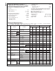


Electrical Characteristics (Continued)
The following specifications apply for Mode 1, Q = 10 (R
1
=R
3
= 100k, R
2
= 10k), V
+
= +5V and V
−
= −5V unless otherwise
specified. Boldface limits apply for T
MIN
to T
MAX
; all other limits T
A
=T
J
= 25˚C.
Symbol Parameter Conditions
LMF100CCN LMF100CIWM
Units
Typical
(Note 8)
Tested
Limit
(Note 9)
Design
Limit
(Note 10)
Typical
(Note 8)
Tested
Limit
(Note 9)
Design
Limit
(Note 10)
I
IN
Input Current on Pins: 4, 5, 10 10 µA
6, 9, 10, 11, 12, 16, 17
Electrical Characteristics
The following specifications apply for Mode 1, Q = 10 (R
1
=R
3
= 100k, R
2
= 10k), V
+
= +2.50V and V
−
= −2.50V unless oth-
erwise specified. Boldface limits apply for T
MIN
to T
MAX
; all other limits T
A
=T
J
= 25˚C.
Symbol Parameter Conditions
LMF100CCN LMF100CIWM
Units
Typical
(Note 8)
Tested
Limit
(Note 9)
Design
Limit
(Note
10)
Typical
(Note 8)
Tested
Limit
(Note 9)
Design
Limit
(Note
10)
I
s
Maximum Supply
Current
f
CLK
= 250 kHz
No Input Signal
81212 8 12 mA
f
0
Center Frequency MIN 0.1 0.1 Hz
Range MAX 50 50 kHz
f
CLK
Clock Frequency MIN 5.0 5.0 Hz
Range MAX 1.5 1.5 MHz
f
CLK
/f
0
Clock to Center V
Pin12
= 2.5V or 0V
±
0.2
±
1
±
1
±
0.2
±
1 %
Frequency Ratio Deviation f
CLK
= 1 MHz
Q Error (MAX) Q = 10, Mode 1
(Note 4) V
Pin12
=5Vor0V
±
0.5
±
5
±
8
±
0.5
±
8 %
f
CLK
= 1 MHz
H
OBP
Bandpass Gain at f
0
f
CLK
= 1 MHz 0
±
0.4
±
0.5 0
±
0.5 dB
H
OLP
DC Lowpass Gain R
1
=R
2
= 10k 0
±
0.2
±
0.2 0
±
0.2 dB
f
CLK
= 250 kHz
V
OS1
DC Offset Voltage (Note 5) f
CLK
= 250 kHz
±
5.0
±
15
±
15
±
5.0
±
15 mV
V
OS2
DC Offset Voltage (Note 5) f
CLK
= 250 kHz S
A/B
=V
+
±
20
±
60
±
60
±
20
±
60 mV
S
A/B
=V
−
±
10
±
50
±
60
±
10
±
60 mV
V
OS3
DC Offset Voltage (Note 5) f
CLK
= 250 kHz
±
10
±
25
±
30
±
10
±
30 mV
Crosstalk (Note 6) A Side to B Side or −65 −65 dB
B Side to A Side
Output Noise (Note 12) f
CLK
= 250 kHz N 25 25
20 kHz Bandwidth BP 250 250 µV
100:1 Mode LP 220 220
Clock Feedthrough (Note 13) f
CLK
= 250 kHz 100:1 Mode 2 2 mV
V
OUT
Minimum Output R
L
= 5k +1.6
±
1.5
±
1.4
+1.6
±
1.4 V
Voltage Swing (All Outputs) −2.2 −2.2
R
L
= 3.5k +1.5 +1.5 V
(All outputs) −2.1 −2.1
GBW Op Amp Gain BW Product 5 5 MHz
SR Op Amp Slew Rate 18 18 V/µs
I
sc
Maximum Output
Short Circuit
Source (All Outputs) 10 10 mA
Current (Note 7) Sink 20 20 mA
LMF100
www.national.com3