
Datasheet


Absolute Maximum Ratings (Note 1)
If Military/Aerospace specified devices are required,
please contact the National Semiconductor Sales Office/
Distributors for availability and specifications.
(Note 14)
Supply Voltage (V
+
−V
−
) 16V
Voltage at Any Pin V
+
+ 0.3V
V
−
− 0.3V
Input Current at Any Pin (Note 2) 5 mA
Package Input Current (Note 2) 20 mA
Power Dissipation (Note 3) 500 mW
Storage Temperature 150˚C
ESD Susceptability (Note 11) 2000V
Soldering Information
N Package: 10 sec. 260˚C
J Package: 10 sec. 300˚C
SO Package:
Vapor Phase (60 sec.) 215˚C
Infrared (15 sec.) 220˚C
See AN-450 “Surface Mounting Methods and Their Effect
on Product Reliability” (Appendix D) for other methods of
soldering surface mount devices.
Operating Ratings (Note 1)
Temperature Range T
MIN
≤ T
A
≤ T
MAX
LMF100CCN 0˚C ≤ T
A
≤ +70˚C
LMF100CIWM −40˚C ≤ T
A
≤ +85˚C
Supply Voltage 4V ≤ V
+
−V
−
≤15V
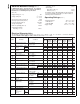
Electrical Characteristics
The following specifications apply for Mode 1, Q = 10 (R
1
=R
3
= 100k, R
2
= 10k), V
+
= +5V and V
−
= −5V unless otherwise
specified. Boldface limits apply for T
MIN
to T
MAX
; all other limits T
A
=T
J
= 25˚C.
Symbol Parameter Conditions
LMF100CCN LMF100CIWM
Units
Typical
(Note 8)
Tested
Limit
(Note 9)
Design
Limit
(Note 10)
Typical
(Note 8)
Tested
Limit
(Note 9)
Design
Limit
(Note 10)
I
s
Maximum Supply Current f
CLK
= 250 kHz 9 13 13 9 13 mA
No Input Signal
f
0
Center Frequency MIN 0.1 0.1 Hz
Range MAX 100 100 kHz
f
CLK
Clock Frequency MIN 5.0 5.0 Hz
Range MAX 3.5 3.5 MHz
f
CLK
/f
0
Clock to Center Frequency
Ratio Deviation
V
Pin12
=5Vor0V
f
CLK
= 1 MHz
±
0.2
±
0.8
±
0.8
±
0.2
±
0.8 %
Q Error (MAX) (Note 4) Q = 10, Mode 1
V
Pin12
=5Vor0V
f
CLK
= 1 MHz
±
0.5
±
5
±
6
±
0.5
±
6 %
H
OBP
Bandpass Gain at f
0
f
CLK
= 1 MHz 0
±
0.4
±
0.4 0
±
0.4 dB
H
OLP
DC Lowpass Gain R
1
=R
2
= 10k 0
±
0.2
±
0.2 0
±
0.2 dB
f
CLK
= 250 kHz
V
OS1
DC Offset Voltage (Note 5) f
CLK
= 250 kHz
±
5.0
±
15
±
15
±
5.0
±
15 mV
V
OS2
DC Offset Voltage (Note 5) f
CLK
= 250 kHz S
A/B
=V
+
±
30
±
80
±
80
±
30
±
80 mV
S
A/B
=V
−
±
15
±
70
±
70
±
15
±
70 mV
V
OS3
DC Offset Voltage (Note 5) f
CLK
= 250 kHz
±
15
±
40
±
60
±
15
±
60 mV
Crosstalk (Note 6) A Side to B Side or
−60 −60 dB
B Side to A Side
Output Noise (Note 12) f
CLK
= 250 kHz N 40 40
20 kHz Bandwidth BP 320 320 µV
100:1 Mode LP 300 300
Clock Feedthrough
(Note 13)
f
CLK
= 250 kHz 100:1 Mode 6 6 mV
V
OUT
Minimum Output R
L
= 5k +4.0
±
3.8
±
3.7
+4.0
±
3.7 V
Voltage Swing (All Outputs) −4.7 −4.7
R
L
= 3.5k +3.9 +3.9
V
(All Outputs) −4.6 −4.6
GBW Op Amp Gain BW Product 5 5 MHz
SR Op Amp Slew Rate 20 20 V/µs
I
sc
Maximum Output
Short
Source (All Outputs) 12 12 mA
Circuit Current
(Note 7)
Sink 45 45 mA
LMF100
www.national.com 2