
Datasheet


LMC6762
www.ti.com
SNOS739D –JULY 1997–REVISED MARCH 2013
A voltage divider of R
4
and R
5
establishes a reference voltage V
1
at the non-inverting input. By making the series
resistance of R
1
and R
2
equal to R
5
, the comparator will switch when V
IN
= 0. Diode D
1
insures that V
3
never
drops below −0.7V. The voltage divider of R
2
and R
3
then prevents V
2
from going below ground. A small amount
of hysteresis is setup to ensure rapid output voltage transitions.
Oscillator
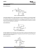
Figure 33. Square Wave Generator
Figure 33 shows the application of the LMC6762 in a square wave generator circuit. The total hysteresis of the
loop is set by R
1
, R
2
and R
3
. R
4
and R
5
provide separate charge and discharge paths for the capacitor C. The
charge path is set through R
4
and D
1
. So, the pulse width t
1
is determined by the RC time constant of R
4
and C.
Similarly, the discharge path for the capacitor is set by R
5
and D
2
. Thus, the time t
2
between the pulses can be
changed by varying R
5
, and the pulse width can be altered by R
4
. The frequency of the output can be changed
by varying both R
4
and R
5
.
Copyright © 1997–2013, Texas Instruments Incorporated Submit Documentation Feedback 13
Product Folder Links: LMC6762