
Datasheet


LMC6572, LMC6574
SNOS707D –DECEMBER 1996–REVISED MARCH 2013
www.ti.com
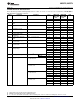
2.7V DC Electrical Characteristics (continued)
Unless otherwise specified, all limits guaranteed for T
J
= 25°C. V
+
= 2.7V, V
−
= 0V, V
CM
= V
O
= V
+
/2 and R
L
> 1MΩ. Boldface
limits apply at the temperature extremes.
Symbol Parameter Conditions Typ
(1)
LMC6574AI LMC6574BI Units
LMC6572AI LMC6572BI
Limit
(2)
Limit
(2)
I
SC
Output Short Circuit Current Sourcing, V
O
= 0V 6.0 4.0 3.0 mA
3.0 2.0 Min
Sinking, V
O
= 2.7V 4.0 3.0 2.5 mA
2.0 1.5 Min
I
S
Supply Current Quad Package 160 240 240 μA
V
+
= +2.7V, V
O
= V
+
/2
280 280 Max
Quad Package 160 240 240 μA
V
+
= +3V, V
O
= V
+
/2
280 280 Max
Dual Package 80 120 120 μA
V
+
= +2.7V, V
O
= V
+
/2
140 140 Max
Dual Package 80 120 120 μA
V
+
= +3V, V
O
= V
+
/2
140 140 Max
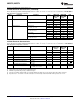
2.7V AC Electrical Characteristics
Unless otherwise specified, all limits guaranteed for T
J
= 25°C, V
+
= 2.7V, V
−
= 0V, V
CM
= V
O
= V
+
/2 and R
L
> 1 MΩ. Boldface
limits apply at the temperature extremes.
Symbol Parameter Conditions Typ
(1)
LMC6574AI LMC6574BI Units
LMC6572AI LMC6572BI
Limit
(2)
Limit
(2)
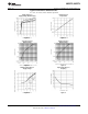
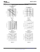
SR Slew Rate V
+
= 2.7V and 3V
(3)
90 30 30 V/ms
10 10 Min
GBW Gain-Bandwidth Product V
+
= 3V 0.22 MHz
φ
m
Phase Margin 60 Deg
G
m
Gain Margin 12 dB
Amp-to-Amp Isolation See
(4)
120 dB
e
n
Input-Referred Voltage Noise F = 1 kHz 45
nV/√Hz
V
CM
= 1V
i
n
Input-Referred Current Noise F = 1 kHz 0.002 pA/√Hz
T.H.D. Total Harmonic Distortion F = 10 kHz, A
V
= −2 0.05
%
R
L
= 10 kΩ, V
O
= 1.0 V
PP
(1) Typical values represent the most likely parametric norm.
(2) All limits are guaranteed by testing or statistical analysis.
(3) Connected as Voltage Follower with 1.0V step input. Number specified is the slower of the positive and negative slew rates.
(4) Input referred, V
+
= 3V and R
L
= 100 kΩ connected to 1.5V. Each amp excited in turn with 1 KHz to produce V
O
= 2 V
PP
.
4 Submit Documentation Feedback Copyright © 1996–2013, Texas Instruments Incorporated
Product Folder Links: LMC6572 LMC6574