
Datasheet


LMC6572, LMC6574
www.ti.com
SNOS707D –DECEMBER 1996–REVISED MARCH 2013
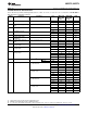
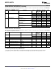
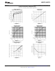
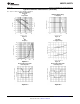
2.7V DC Electrical Characteristics
Unless otherwise specified, all limits guaranteed for T
J
= 25°C. V
+
= 2.7V, V
−
= 0V, V
CM
= V
O
= V
+
/2 and R
L
> 1MΩ. Boldface
limits apply at the temperature extremes.
Symbol Parameter Conditions Typ
(1)
LMC6574AI LMC6574BI Units
LMC6572AI LMC6572BI
Limit
(2)
Limit
(2)
V
OS
Input Offset Voltage V
+
= 2.7V and 3V 0.5 3 7 mV
3.5 7.5 Max
TCV
OS
Input Offset Voltage Average 1.5 μV/°C
Drift
I
B
Input Current 0.02 pA
10 10 Max
I
OS
Input Offset Current 0.01 pA
6 6 Max
R
IN
Input Resistance >1 Tera Ω
C
IN
Common-Mode Input 3 pF
Capacitance
CMRR Common Mode Rejection 0V ≤ V
CM
≤ 3.5V V
+
= 5V 75 63 60 dB
Ratio
60 57 Min
+PSRR Positive Power Supply 2.7V ≤ V
+
≤ 5V, V
−
= 0V 75 67 60 dB
Rejection Ratio
65 58 Min
−PSRR Negative Power Supply −2.7V ≤ V
−
≤ −5V, V
+
= 0V 83 75 67 dB
Rejection Ratio
73 65 Min
V
CM
Input Common-Mode V
+
= 2.7V and 3V for CMRR ≥ 50 dB −0.1 −0.05 −0.05 V
Voltage Range
0 0 Max
V
+
− 0.8 V
+
− 1.0 V
+
− 1.0 V
V
+
− 1.3 V
+
− 1.3 Min
A
V
Large Signal Voltage Gain R
L
= 100 kΩ
(3)
Sourcing 1000 V/mV
Sinking 500 V/mV
V
O
Output Swing V
+
= 2.7V 2.695 2.68 2.65 V
R
L
= 100 kΩ to V
+
/2
2.66 2.62 Min
0.005 0.03 0.06 V
0.05 0.09 Max
V
+
= 2.7V 2.66 2.55 2.45 V
R
L
= 5 kΩ to V
+
/2
2.45 2.35 Min
0.04 0.15 0.25 V
0.25 0.35 Max
V
+
= 3V 2.995 2.98 2.95 V
R
L
= 100 kΩ to V
+
/2
2.96 2.93 Min
0.005 0.03 0.06 V
0.05 0.09 Max
V
+
= 3V 2.96 2.85 2.75 V
R
L
= 5 kΩ to V
+
/2
2.75 2.65 Min
0.04 0.15 0.25 V
0.25 0.35 Max
(1) Typical values represent the most likely parametric norm.
(2) All limits are guaranteed by testing or statistical analysis.
(3) V
+
= 3V, V
CM
= 1.5V and R
L
connected to 1.5V. For Sourcing tests, 1.5V ≤ V
O
≤ 2.5V. For Sinking tests, 0.5V ≤ V
O
≤ 1.5V.
Copyright © 1996–2013, Texas Instruments Incorporated Submit Documentation Feedback 3
Product Folder Links: LMC6572 LMC6574