
Datasheet


Table Of Contents
- FEATURES
- APPLICATIONS
- DESCRIPTION
- Absolute Maximum Ratings
- Operating Ratings
- DC Electrical Characteristics
- AC Electrical Characteristics
- DC Electrical Characteristics
- AC Electrical Characteristics
- Typical Performance Characteristics
- Application Information
- AMPLIFIER TOPOLOGY
- INPUT COMMON-MODE VOLTAGE RANGE
- RAIL-TO-RAIL OUTPUT
- CAPACITIVE LOAD TOLERANCE
- COMPENSATING FOR INPUT CAPACITANCE
- PRINTED-CIRCUIT-BOARD LAYOUT FOR HIGH-IMPEDANCE WORK
- OFFSET VOLTAGE ADJUSTMENT
- UPGRADING APPLICATIONS
- DATA ACQUISITION SYSTEMS
- INSTRUMENTATION CIRCUITS
- SPICE MACROMODEL
- Typical Single-Supply Applications
- Revision History
LMC6482
www.ti.com
SNOS674D –NOVEMBER 1997–REVISED MARCH 2013
AC Electrical Characteristics (continued)
Unless otherwise specified, all limits specified for T
J
= 25°C, V
+
= 5V, V
−
= 0V, V
CM
= V
O
= V
+
/2, and R
L
> 1M. Boldface limits
apply at the temperature extremes.
LMC6482AI LMC6482I LMC6482M
Typ
Parameter Test Conditions Limit Limit Limit Units
(1)
(2) (2) (2)
G
m
Gain Margin 15 dB
Amp-to-Amp Isolation
(4)
150 dB
e
n
Input-Referred Voltage Noise F = 1kHz 37
nV/√Hz
V
cm
= 1V
I
n
Input-Referred Current Noise F = 1kHz 0.03 pA/√Hz
T.H.D. Total Harmonic Distortion F = 10kHz, A
V
= −2 0.01
%
R
L
= 10kΩ, V
O
= 4.1 V
PP
F = 10kHz, A
V
= −2 0.01 %
R
L
= 10kΩ, V
O
= 8.5 V
PP
V
+
= 10V
(4) Input referred, V
+
= 15V and R
L
= 100 kΩ connected to 7.5V. Each amp excited in turn with 1 kHz to produce V
O
= 12 V
PP
.
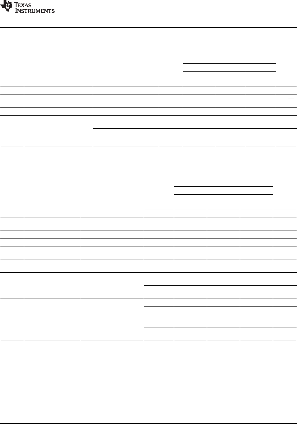
DC Electrical Characteristics
Unless otherwise specified, all limits specified for T
J
= 25°C, V
+
= 3V, V
−
= 0V, V
CM
= V
O
= V
+
/2 and R
L
> 1M.
LMC6482AI LMC6482I LMC6482M
Typ
Parameter Test Conditions Limit Limit Limit Units
(1)
(2) (2) (2)
V
OS
Input Offset Voltage 0.9 2.0 3.0 3.0 mV
2.7 3.7 3.8 max
TCV
OS
Input Offset Voltage
2.0 μV/°C
Average Drift
I
B
Input Bias Current 0.02 pA
I
OS
Input Offset Current 0.01 pA
CMRR Common Mode Rejection 0V ≤ V
CM
≤ 3V 74 64 60 60 dB
Ratio min
PSRR Power Supply Rejection 3V ≤ V
+
≤ 15V, V
−
= 0V 80 68 60 60 dB
Ratio min
V
CM
Input Common-Mode For CMRR ≥ 50dB V
−
−0.25 0 0 0 V
Voltage Range max
V
+
+ 0.25 V
+
V
+
V
+
V
min
V
O
Output Swing R
L
= 2kΩ to V
+
/2 2.8 V
0.2 V
R
L
= 600Ω to V
+
/2 2.7 2.5 2.5 2.5 V
min
0.37 0.6 0.6 0.6 V
max
I
S
Supply Current Both Amplifiers 0.825 1.2 1.2 1.2 mA
1.5 1.5 1.6 max
(1) Typical Values represent the most likely parametric norm.
(2) All limits are specified by testing or statistical analysis.
Copyright © 1997–2013, Texas Instruments Incorporated Submit Documentation Feedback 5
Product Folder Links: LMC6482