
Datasheet


Table Of Contents
- FEATURES
- APPLICATIONS
- DESCRIPTION
- Absolute Maximum Ratings
- Operating Ratings
- DC Electrical Characteristics
- AC Electrical Characteristics
- DC Electrical Characteristics
- AC Electrical Characteristics
- Typical Performance Characteristics
- Application Information
- AMPLIFIER TOPOLOGY
- INPUT COMMON-MODE VOLTAGE RANGE
- RAIL-TO-RAIL OUTPUT
- CAPACITIVE LOAD TOLERANCE
- COMPENSATING FOR INPUT CAPACITANCE
- PRINTED-CIRCUIT-BOARD LAYOUT FOR HIGH-IMPEDANCE WORK
- OFFSET VOLTAGE ADJUSTMENT
- UPGRADING APPLICATIONS
- DATA ACQUISITION SYSTEMS
- INSTRUMENTATION CIRCUITS
- SPICE MACROMODEL
- Typical Single-Supply Applications
- Revision History
LMC6482
www.ti.com
SNOS674D –NOVEMBER 1997–REVISED MARCH 2013
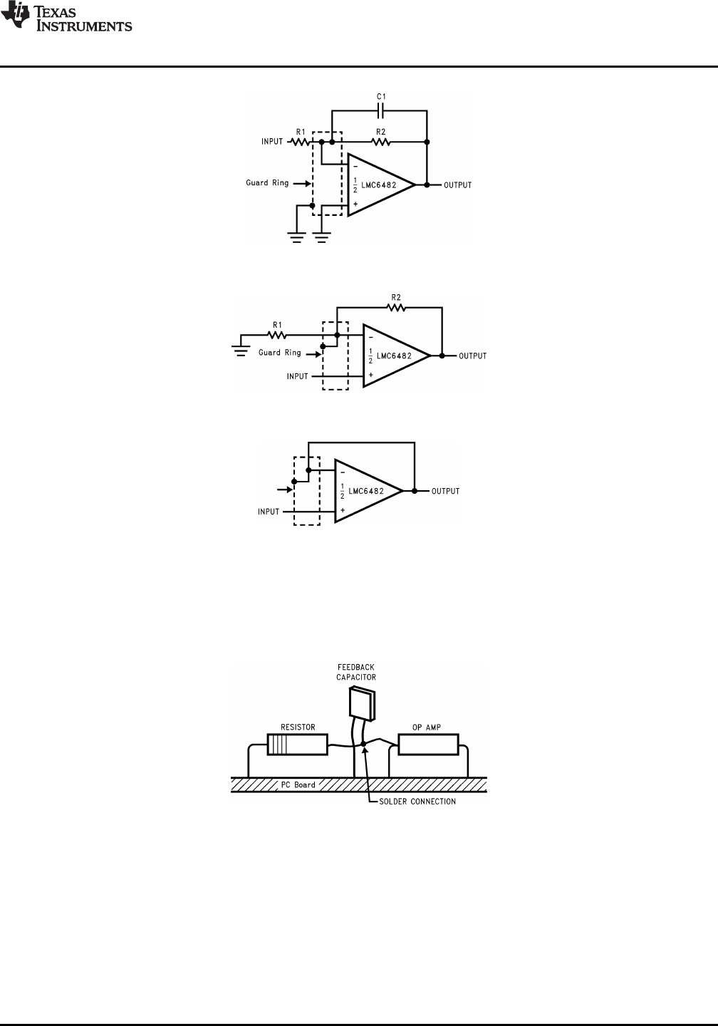
Figure 65. Inverting Amplifier Typical Connections of Guard Rings
Figure 66. Non-Inverting Amplifier Typical Connections of Guard Rings
Figure 67. Follower Typical Connections of Guard Rings
The designer should be aware that when it is inappropriate to lay out a PC board for the sake of just a few
circuits, there is another technique which is even better than a guard ring on a PC board: Don't insert the
amplifier's input pin into the board at all, but bend it up in the air and use only air as an insulator. Air is an
excellent insulator. In this case you may have to forego some of the advantages of PC board construction, but
the advantages are sometimes well worth the effort of using point-to-point up-in-the-air wiring. See Figure 68.
(Input pins are lifted out of PC board and soldered directly to components. All other pins connected to PC board.)
Figure 68. Air Wiring
OFFSET VOLTAGE ADJUSTMENT
Offset voltage adjustment circuits are illustrated in Figure 69 and Figure 70. Large value resistances and
potentiometers are used to reduce power consumption while providing typically ±2.5mV of adjustment range,
referred to the input, for both configurations with V
S
= ±5V.
Copyright © 1997–2013, Texas Instruments Incorporated Submit Documentation Feedback 21
Product Folder Links: LMC6482