
Datasheet


Table Of Contents
- FEATURES
- APPLICATIONS
- DESCRIPTION
- Absolute Maximum Ratings
- Operating Ratings
- DC Electrical Characteristics
- AC Electrical Characteristics
- DC Electrical Characteristics
- AC Electrical Characteristics
- Typical Performance Characteristics
- Application Information
- AMPLIFIER TOPOLOGY
- INPUT COMMON-MODE VOLTAGE RANGE
- RAIL-TO-RAIL OUTPUT
- CAPACITIVE LOAD TOLERANCE
- COMPENSATING FOR INPUT CAPACITANCE
- PRINTED-CIRCUIT-BOARD LAYOUT FOR HIGH-IMPEDANCE WORK
- OFFSET VOLTAGE ADJUSTMENT
- UPGRADING APPLICATIONS
- DATA ACQUISITION SYSTEMS
- INSTRUMENTATION CIRCUITS
- SPICE MACROMODEL
- Typical Single-Supply Applications
- Revision History
LMC6482
SNOS674D –NOVEMBER 1997–REVISED MARCH 2013
www.ti.com
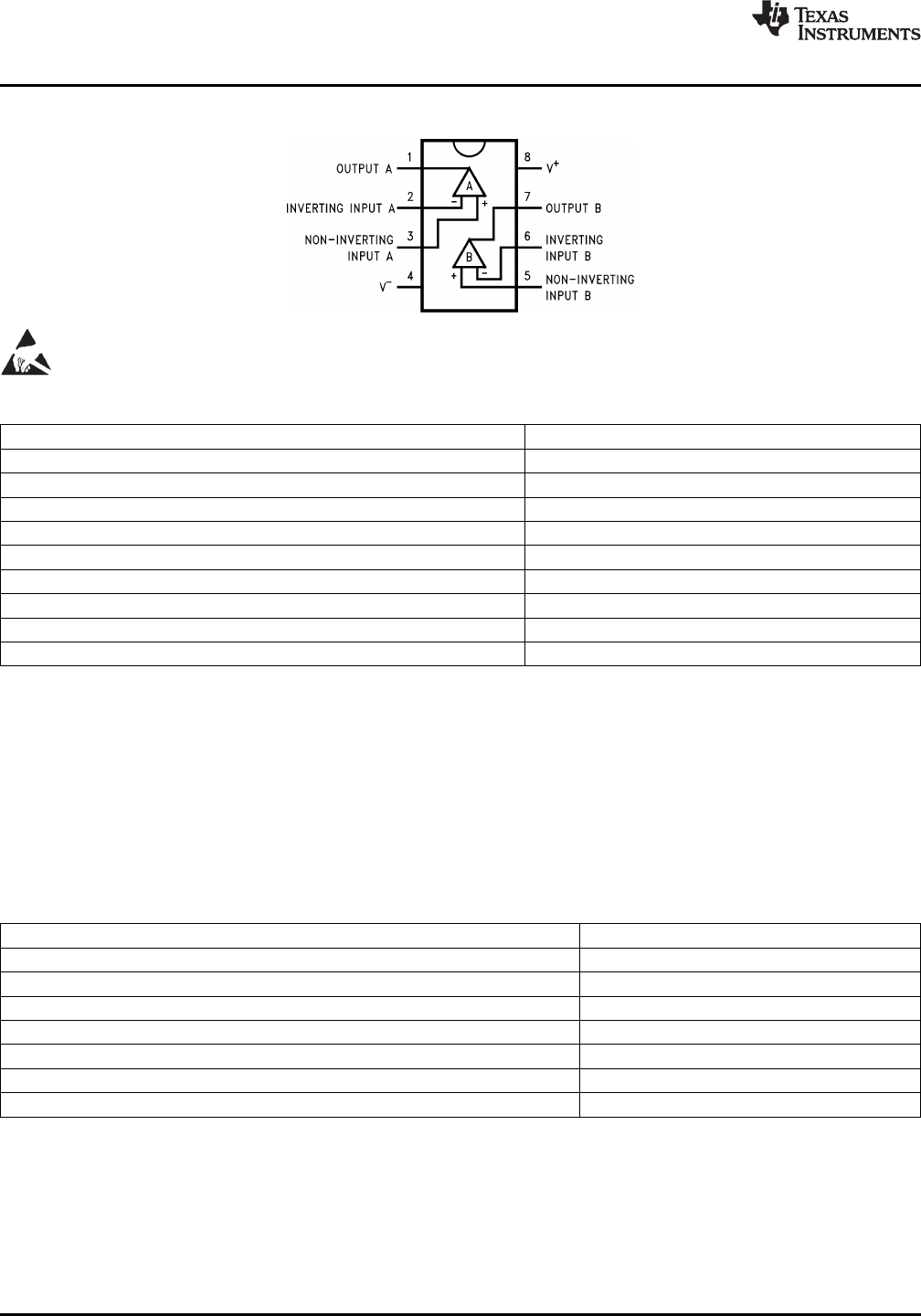
Connection Diagram
These devices have limited built-in ESD protection. The leads should be shorted together or the device placed in conductive foam
during storage or handling to prevent electrostatic damage to the MOS gates.
Absolute Maximum Ratings
(1)(2)
ESD Tolerance
(3)
1.5kV
Differential Input Voltage ±Supply Voltage
Voltage at Input/Output Pin (V
+
) +0.3V, (V
−
) −0.3V
Supply Voltage (V
+
− V
−
) 16V
Current at Input Pin
(4)
±5mA
Current at Output Pin
(5) (6)
±30mA
Current at Power Supply Pin 40mA
Lead Temperature (Soldering, 10 sec.) 260°C
Storage Temperature Range −65°C to +150°C
Junction Temperature
(7)
150°C
(1) Absolute Maximum Ratings indicate limits beyond which damage to the device may occur. Operating Ratings indicate conditions for
which the device is intended to be functional, but specific performance is not ensured. For ensured specifications and the test
conditions, see the Electrical Characteristics.
(2) If Military/Aerospace specified devices are required, please contact the TI Sales Office/Distributors for availability and specifications.
(3) Human body model, 1.5kΩ in series with 100pF. All pins rated per method 3015.6 of MIL-STD-883. This is a Class 1 device rating.
(4) Limiting input pin current is only necessary for input voltages that exceed absolute maximum input voltage ratings.
(5) Applies to both single-supply and split-supply operation. Continuous short circuit operation at elevated ambient temperature can result in
exceeding the maximum allowed junction temperature of 150°C. Output currents in excess of ±30mA over long term may adversely
affect reliability.
(6) Do not short circuit output to V
+
, when V
+
is greater than 13V or reliability will be adversely affected.
(7) The maximum power dissipation is a function of T
J(max)
, θ
JA
, and T
A
. The maximum allowable power dissipation at any ambient
temperature is P
D
= (T
J(max)
− T
A
)/θ
JA
. All numbers apply for packages soldered directly into a PC board.
Operating Ratings
Supply Voltage 3.0V ≤ V+ ≤ 15.5V
Junction Temperature Range
LMC6482AM −55°C ≤ T
J
≤ +125°C
LMC6482AI, LMC6482I −40°C ≤ T
J
≤ +85°C
Thermal Resistance (θ
JA
)
P0008E Package, 8-Pin PDIP 90°C/W
D0008A Package, 8-Pin SOIC 155°C/W
DGK0008A Package, 8-Pin VSSOP 194°C/W
(1) Absolute Maximum Ratings indicate limits beyond which damage to the device may occur. Operating Ratings indicate conditions for
which the device is intended to be functional, but specific performance is not ensured. For ensured specifications and the test
conditions, see the Electrical Characteristics.
2 Submit Documentation Feedback Copyright © 1997–2013, Texas Instruments Incorporated
Product Folder Links: LMC6482