
Datasheet


LMC6462, LMC6464
www.ti.com
SNOS725D –MAY 1999–REVISED MARCH 2013
Then,
(7)
(8)
= 1 Hz
Low Frequency Null
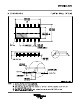
Figure 56. High Gain Amplifier with Low Frequency Null
Output offset voltage is the error introduced in the output voltage due to the inherent input offset voltage V
OS
, of
an amplifier.
Output Offset Voltage = (Input Offset Voltage) (Gain)
In the above configuration, the resistors R
5
and R
6
determine the nominal voltage around which the input signal,
V
IN
should be symmetrical. The high frequency component of the input signal V
IN
will be unaffected while the low
frequency component will be nulled since the DC level of the output will be the input offset voltage of the
LMC6462 plus the bias voltage. This implies that the output offset voltage due to the top amplifier will be
eliminated.
Copyright © 1999–2013, Texas Instruments Incorporated Submit Documentation Feedback 21
Product Folder Links: LMC6462 LMC6464