
Datasheet
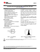


LMC6061
www.ti.com
SNOS648D –NOVEMBER 1994–REVISED MARCH 2013
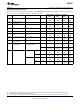
DC Electrical Characteristics
Unless otherwise specified, all limits ensured for T
J
= 25°C. Boldface limits apply at the temperature extremes. V
+
= 5V, V
−
=
0V, V
CM
= 1.5V, V
O
= 2.5V and R
L
> 1M unless otherwise specified.
LMC6061AM LMC6061AI LMC6061I
Symbol Parameter Conditions Typ
(1)
Units
Limit
(2)
Limit
(2)
Limit
(2)
V
OS
Input Offset Voltage 100 350 350 800 μV
1200 900 1300 Max
TCV
OS
Input Offset Voltage 1.0 μV/°C
Average Drift
I
B
Input Bias Current 0.010 pA
100 4 4 Max
I
OS
Input Offset Current 0.005 pA
100 2 2 Max
R
IN
Input Resistance >10 Tera Ω
CMRR Common Mode Rejection 0V ≤ V
CM
≤ 12.0V 85 75 75 66 dB
Ratio V
+
= 15V
70 72 63 Min
+PSRR Positive Power Supply 5V ≤ V
+
≤ 15V 85 75 75 66 dB
Rejection Ratio V
O
= 2.5V
70 72 63 Min
−PSRR Negative Power Supply 0V ≤ V
−
≤ −10V 100 84 84 74 dB
Rejection Ratio
70 81 71 Min
V
CM
Input Common-Mode V
+
= 5V and 15V −0.4 −0.1 −0.1 −0.1 V
Voltage Range for CMRR ≥ 60 dB
0 0 0 Max
V
+
− 1.9 V
+
− 2.3 V
+
− 2.3 V
+
− 2.3 V
V
+
− 2.6 V
+
− 2.5 V
+
− 2.5 Min
A
V
Large Signal Voltage Gain R
L
= 100 kΩ
(3)
Sourcing 4000 400 400 300 V/mV
200 300 200 Min
Sinking 3000 180 180 90 V/mV
70 100 60 Min
R
L
= 25 kΩ
(3)
Sourcing 3000 400 400 200 V/mV
150 150 80 Min
Sinking 2000 100 100 70 V/mV
35 50 35 Min
(1) For operating at elevated temperatures the device must be derated based on the thermal resistance θ
JA
with P
D
= (T
J
–T
A
)/θ
JA
(2) All limits are specified by testing or statistical analysis.
(3) V
+
= 15V, V
CM
= 7.5V and R
L
connected to 7.5V. For Sourcing tests, 7.5V ≤ V
O
≤ 11.5V. For Sinking tests, 2.5V ≤ V
O
≤ 7.5V.
Copyright © 1994–2013, Texas Instruments Incorporated Submit Documentation Feedback 3
Product Folder Links: LMC6061