
Datasheet
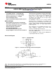


LMC6042
SNOS611E –AUGUST 1999–REVISED MARCH 2013
www.ti.com
This integrated circuit can be damaged by ESD. Texas Instruments recommends that all integrated circuits be handled with
appropriate precautions. Failure to observe proper handling and installation procedures can cause damage.
ESD damage can range from subtle performance degradation to complete device failure. Precision integrated circuits may be more
susceptible to damage because very small parametric changes could cause the device not to meet its published specifications.
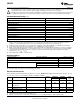
Absolute Maximum Ratings
(1)(2)
Differential Input Voltage ±Supply Voltage
Supply Voltage (V
+
− V
−
) 16V
Output Short Circuit to V
+
See
(3)
Output Short Circuit to V
−
See
(4)
Lead Temperature (Soldering, 10 seconds) 260°C
Current at Input Pin ±5 mA
Current at Output Pin ±18 mA
Current at Power Supply Pin 35 mA
Power Dissipation See
(5)
Storage Temperature Range −65°C to +150°C
Junction Temperature
(5)
110°C
ESD Tolerance
(6)
500V
Voltage at Input/Output Pin (V
+
) + 0.3V, (V
−
) − 0.3V
(1) Absolute Maximum Ratings indicate limits beyond which damage to the device may occur. Operating Conditions indicate conditions for
which the device is intended to be functional, but do not ensure specific performance limits. For ensured specifications and test
conditions, see the Electrical Characteristics. The ensured specifications apply only for the test conditions listed.
(2) If Military/Aerospace specified devices are required, please contact the TI Sales Office/Distributors for availability and specifications.
(3) Do not connect output to V
+
when V
+
is greater than 13V or reliability may be adversely affected.
(4) Applies to both single-supply operation. Continuous short circuit operation at elevated ambient temperature can result in exceeding the
maximum allowed junction temperature of 110°C. Output currents in excess of ±30 mA over long term may adversely affect reliability.
(5) The maximum power dissipation is a function of T
J(Max)
, θ
JA
, and T
A
. The maximum allowable power dissipation at any ambient
temperature is P
D
= (T
J(Max)
− T
A
)/θ
JA
.
(6) Human body model, 1.5 kΩ in series with 100 pF.
Operating Ratings
Temperature Range LMC6042AI, LMC6042I −40°C ≤ T
J
≤ +85°C
Supply Voltage 4.5V ≤ V
+
≤ 15.5V
Power Dissipation See
(1)
Thermal Resistance (θ
JA
),
(2)
8-Pin PDIP 101°C/W
8-Pin SOIC 165°C/W
8-Pin CDIP 115°C/W
(1) For operating at elevated temperatures the device must be derated based on the thermal resistance θ
JA
with P
D
= (T
J
− T
A
)/θ
JA
.
(2) All numbers apply for packages soldered directly into a PC board.
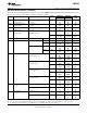
Electrical Characteristics
Unless otherwise specified, all limits ensured for T
A
= T
J
= 25°C. Boldface limits apply at the temperature extremes. V
+
= 5V,
V
−
= 0V, V
CM
= 1.5V, V
O
= V
+
/2 and R
L
> 1M unless otherwise specified.
Typical
(1)
LMC6042AI LMC6042I Units
Symbol Parameter Conditions
(Limit)
Limit
(2)
Limit
(2)
V
OS
Input Offset Voltage 1 3 6 mV
3.3 6.3 Max
TCV
OS
Input Offset Voltage 1.3 μV/°C
Average Drift
I
B
Input Bias Current 0.002 4 4 pA (Max)
I
OS
Input Offset Current 0.001 2 2 pA (Max)
R
IN
Input Resistance >10 TeraΩ
(1) Typical values represent the most likely parametric norm.
(2) All limits are specified at room temperature (standard type face) or at operating temperature extremes (bold face type).
2 Submit Documentation Feedback Copyright © 1999–2013, Texas Instruments Incorporated
Product Folder Links: LMC6042