
Datasheet


LMC6035, LMC6035-Q1, LMC6036
www.ti.com
SNOS875G –JANUARY 2000–REVISED APRIL 2013
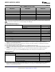
DC Electrical Characteristics
Unless otherwise specified, all limits ensured for T
J
= 25°C, V
+
= 2.7V, V
−
= 0V, V
CM
= 1.0V, V
O
= 1.35V and R
L
> 1MΩ.
Boldface limits apply at the temperature extremes.
LMC6035I/LMC6036I
Parameter Test Conditions Units
Min
(1)
Typ
(2)
Max
(1)
V
OS
Input Offset Voltage 0.5 5 mV
6
TCV
OS
Input Offset Voltage
2.3 μV/°C
Average Drift
I
IN
Input Current See
(3)
0.02 90 pA
I
OS
Input Offset Current See
(3)
0.01 45 PA
R
IN
Input Resistance > 10 Tera Ω
CMRR Common Mode Rejection Ratio 0.7V ≤ V
CM
≤ 12.7V, 63 96 dB
V
+
= 15V 60
+PSRR Positive Power Supply 5V ≤ V
+
≤ 15V, 63 93 dB
Rejection Ratio V
O
= 2.5V 60
−PSRR Negative Power Supply 0V ≤ V
−
≤ −10V, 74 97 dB
Rejection Ratio V
O
= 2.5V, V
+
= 5V 70
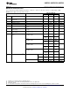
V
CM
Input Common-Mode Voltage V
+
= 2.7V −0.1 0.3
Range For CMRR ≥ 40dB 0.5
V
2.0 2.3
1.7
V
+
= 3V −0.3 0.1
For CMRR ≥ 40dB 0.3
V
2.3 2.6
2.0
V
+
= 5V −0.5 −0.2
For CMRR ≥ 50dB 0.0
V
4.2 4.5
3.9
V
+
= 15V −0.5 −0.2
For CMRR ≥ 50dB 0.0
V
14.0 14.4
13.7
A
V
Large Signal Voltage Gain
(4)
R
L
= 600Ω Sourcing 100 1000 V/mV
75
Sinking 25 250 V/mV
20
R
L
= 2kΩ Sourcing 2000 V/mV
Sinking 500 V/mV
(1) All limits are specified by testing or statistical analysis.
(2) Typical Values represent the most likely parametric norm or one sigma value.
(3) Ensured by design.
(4) V
+
= 15V, V
CM
= 7.5V and R
L
connected to 7.5V. For Sourcing tests, 7.5V ≤ V
O
≤ 11.5V. For Sinking tests, 3.5V ≤ V
O
≤ 7.5V.
Copyright © 2000–2013, Texas Instruments Incorporated Submit Documentation Feedback 3
Product Folder Links: LMC6035 LMC6035-Q1 LMC6036