
Datasheet


LMC6032
www.ti.com
SNOS609C –NOVEMBER 1994–REVISED MARCH 2013
APPLICATION HINTS
AMPLIFIER TOPOLOGY
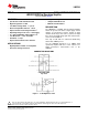
The topology chosen for the LMC6032, shown in Figure 15, is unconventional (compared to general-purpose op
amps) in that the traditional unity-gain buffer output stage is not used; instead, the output is taken directly from
the output of the integrator, to allow a larger output swing. Since the buffer traditionally delivers the power to the
load, while maintaining high op amp gain and stability, and must withstand shorts to either rail, these tasks now
fall to the integrator.
As a result of these demands, the integrator is a compound affair with an embedded gain stage that is doubly fed
forward (via C
f
and C
ff
) by a dedicated unity-gain compensation driver. In addition, the output portion of the
integrator is a push-pull configuration for delivering heavy loads. While sinking current the whole amplifier path
consists of three gain stages with one stage fed forward, whereas while sourcing the path contains four gain
stages with two fed forward.
Figure 15. LMC6032 Circuit Topology (Each Amplifier)
The large signal voltage gain while sourcing is comparable to traditional bipolar op amps, even with a 600Ω load.
The gain while sinking is higher than most CMOS op amps, due to the additional gain stage; however, under
heavy load (600Ω) the gain will be reduced as indicated in the Electrical Characteristics.
COMPENSATING INPUT CAPACITANCE
The high input resistance of the LMC6032 op amps allows the use of large feedback and source resistor values
without losing gain accuracy due to loading. However, the circuit will be especially sensitive to its layout when
these large-value resistors are used.
Every amplifier has some capacitance between each input and AC ground, and also some differential
capacitance between the inputs. When the feedback network around an amplifier is resistive, this input
capacitance (along with any additional capacitance due to circuit board traces, the socket, etc.) and the feedback
resistors create a pole in the feedback path. In the following General Operational Amplifier Circuit, Figure 16, the
frequency of this pole is
where C
S
is the total capacitance at the inverting input, including amplifier input capacitance and any stray
capacitance from the IC socket (if one is used), circuit board traces, etc., and R
P
is the parallel combination of R
F
and R
IN
. This formula, as well as all formulae derived below, apply to inverting and non-inverting op-amp
configurations.
When the feedback resistors are smaller than a few kΩ, the frequency of the feedback pole will be quite high,
since C
S
is generally less than 10 pF. If the frequency of the feedback pole is much higher than the “ideal” closed-
loop bandwidth (the nominal closed-loop bandwidth in the absence of C
S
), the pole will have a negligible effect
on stability, as it will add only a small amount of phase shift.
However, if the feedback pole is less than approximately 6 to 10 times the “ideal” −3 dB frequency, a feedback
capacitor, C
F
, should be connected between the output and the inverting input of the op amp. This condition can
also be stated in terms of the amplifier's low-frequency noise gain: To maintain stability, a feedback capacitor will
probably be needed if
Copyright © 1994–2013, Texas Instruments Incorporated Submit Documentation Feedback 9
Product Folder Links: LMC6032