
Datasheet
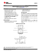


LMC6032
www.ti.com
SNOS609C –NOVEMBER 1994–REVISED MARCH 2013
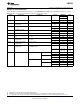
DC Electrical Characteristics
Unless otherwise specified, all limits ensured for T
J
= 25°C. Boldface limits apply at the temperature extremes. V
+
= 5V, V
−
=
GND = 0V, V
CM
= 1.5V, V
OUT
= 2.5V and R
L
> 1M unless otherwise specified.
Symbol Parameter Conditions Typical LMC6032I Units
(1)
Limit
(2)
V
OS
Input Offset Voltage 1 9 mV
11 max
ΔV
OS
/ΔT Input Offset Voltage
2.3 μV/°C
Average Drift
I
B
Input Bias Current 0.04 pA
200 max
I
OS
Input Offset Current 0.01 pA
100 max
R
IN
Input Resistance >1 TeraΩ
CMRR Common Mode Rejection 0V ≤ V
CM
≤ 12V 83 63 dB
Ratio V
+
= 15V
60 min
+PSRR Positive Power Supply 5V ≤ V
+
≤ 15V 83 63 dB
Rejection Ratio V
O
= 2.5V
60 min
−PSRR Negative Power Supply 0V ≤ V
−
≤ −10V 94 74 dB
Rejection Ratio
70 min
V
CM
Input Common-Mode V
+
= 5V & 15V −0.4 −0.1 V
Voltage Range For CMRR ≥ 50 dB
0 max
V
+
− 1.9 V
+
− 2.3 V
V
+
− 2.6 min
A
V
Large Signal Voltage Gain R
L
= 2 kΩ
(3)
Sourcing 2000 200 V/mV
100 min
Sinking 500 90 V/mV
40 min
R
L
= 600Ω
(3)
Sourcing 1000 100 V/mV
75 min
Sinking 250 50 V/mV
20 min
(1) Typical values represent the most likely parametric normal.
(2) All limits are specified at room temperature (standard type face) or at operating temperature extremes (bold type face).
(3) V
+
= 15V, V
CM
= 7.5V, and R
L
connected to 7.5V. For Sourcing tests, 7.5V ≤ V
O
≤ 11.5V. For Sinking tests, 2.5V ≤ V
O
≤ 7.5V.
Copyright © 1994–2013, Texas Instruments Incorporated Submit Documentation Feedback 3
Product Folder Links: LMC6032