
Datasheet


Table Of Contents
- FEATURES
- Applications
- Key Specifications
- DESCRIPTION
- Absolute Maximum Ratings
- Operating Ratings
- Temperature-to-Digital Converter Characteristics
- Logic Electrical Characteristics
- SMBus DIGITAL SWITCHING CHARACTERISTICS
- Functional Description
- CONVERSION SEQUENCE
- THE ALERT OUTPUT
- T_CRIT_A OUTPUT and T_CRIT LIMIT
- POWER ON RESET DEFAULT STATES
- SMBus INTERFACE
- TEMPERATURE DATA FORMAT
- OPEN-DRAIN OUTPUTS
- DIODE FAULT DETECTION
- COMMUNICATING with the LM90
- SERIAL INTERFACE RESET
- DIGITAL FILTER
- Fault Queue
- One-Shot Register
- LM90 REGISTERS
- COMMAND REGISTER
- LOCAL and REMOTE TEMPERATURE REGISTERS (LT, RTHB, RTLB)
- STATUS REGISTER (SR)
- CONFIGURATION REGISTER
- CONVERSION RATE REGISTER
- LOCAL and REMOTE HIGH SETPOINT REGISTERS (LHS, RHSHB, and RHSLB)
- LOCAL and REMOTE LOW SETPOINT REGISTERS (LLS, RLSHB, and RLSLB)
- REMOTE TEMPERATURE OFFSET REGISTERS (RTOHB and RTOLB)
- LOCAL and REMOTE T_CRIT REGISTERS (RCS and LCS)
- T_CRIT HYSTERESIS REGISTER (TH)
- FILTER and ALERT CONFIGURE REGISTER
- MANUFACTURERS ID REGISTER
- DIE REVISION CODE REGISTER
- Application Hints
- Revision History
LM90
www.ti.com
SNIS126A –MAY 2004–REVISED MARCH 2013
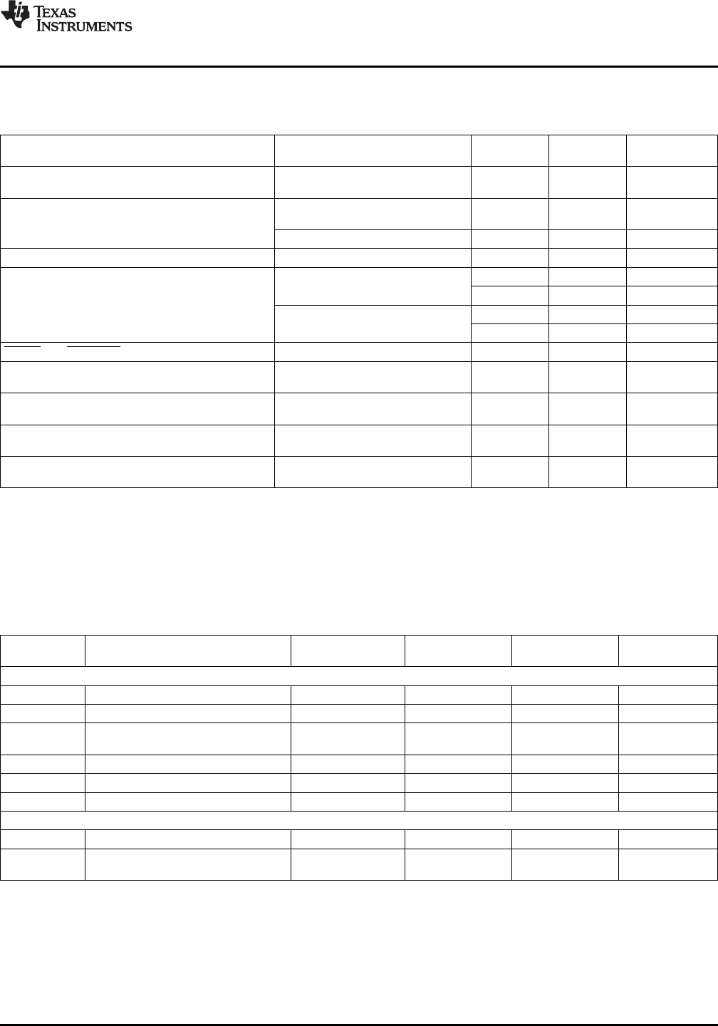
Temperature-to-Digital Converter Characteristics (continued)
Unless otherwise noted, these specifications apply for V
DD
= +3.0Vdc to 3.6Vdc. Boldface limits apply for T
A
= T
J
= T
MIN
≤
T
A
≤ T
MAX
; all other limits T
A
= T
J
= +25°C, unless otherwise noted.
Typical
(1)
Limits
(2)
Units
Parameter Conditions
(Limit)
Conversion Time of All Temperatures at the Fastest See
(4)
31.25 34.4 ms (max)
Setting
Quiescent Current
(5)
SMBus Inactive, 16Hz conversion 0.8 1.7 mA (max)
rate
Shutdown 315 µA
D− Source Voltage 0.7 V
Diode Source Current (D+ − D−)=+ 0.65V; high level 160 315 µA (max)
110 µA (min)
Low level 13 20 µA (max)
7 µA (min)
ALERT and T_CRIT_A Output Saturation Voltage I
OUT
= 6.0 mA 0.4 V (max)
Power-On Reset Threshold Measure on V
DD
input, falling edge 2.4 V (max)
1.8 V (min)
Local and Remote HIGH Default Temperature See
(6)
+70 °C
settings
Local and Remote LOW Default Temperature See
(6)
0 °C
settings
Local and Remote T_CRIT Default Temperature See
(6)
+85 °C
Setting
(4) This specification is provided only to indicate how often temperature data is updated. The LM90 can be read at any time without regard
to conversion state (and will yield last conversion result).
(5) Quiescent current will not increase substantially with an SMBus.
(6) Default values set at power up.
Logic Electrical Characteristics
DIGITAL DC CHARACTERISTICS
Unless otherwise noted, these specifications apply for V
DD
= +3.0 to 3.6 Vdc. Boldface limits apply for T
A
= T
J
= T
MIN
to
T
MAX
; all other limits T
A
= T
J
= +25°C, unless otherwise noted.
Typical
(1)
Limits
(2)
Units
Symbol Parameter Conditions
(Limit)
SMBData, SMBCLK INPUTS
V
IN(1)
Logical “1” Input Voltage 2.1 V (min)
V
IN(0)
Logical “0”Input Voltage 0.8 V (max)
V
IN(HYST)
SMBData and SMBCLK Digital Input 400 mV
Hysteresis
I
IN(1)
Logical “1” Input Current V
IN
= V
DD
0.005 ±10 µA (max)
I
IN(0)
Logical “0” Input Current V
IN
= 0 V −0.005 ±10 µA (max)
C
IN
Input Capacitance 5 pF
ALL DIGITAL OUTPUTS
I
OH
High Level Output Current V
OH
= V
DD
10 µA (max)
V
OL
SMBus Low Level Output Voltage I
OL
= 4mA 0.4 V (max)
I
OL
= 6mA 0.6
(1) Typicals are at T
A
= 25°C and represent most likely parametric norm.
(2) Limits are ensured to AOQL (Average Outgoing Quality Level).
Copyright © 2004–2013, Texas Instruments Incorporated Submit Documentation Feedback 5
Product Folder Links: LM90