
Datasheet


Table Of Contents
- Features
- Applications
- Key Specifications
- Description
- Absolute Maximum Ratings
- Operating Ratings
- Temperature-to-Digital Converter Characteristics
- Logic Electrical Characteristics
- DIGITAL DC CHARACTERISTICS
- SMBus DIGITAL SWITCHING CHARACTERISTICS
- Functional Description
- LM86 REGISTERS
- COMMAND REGISTER
- LOCAL and REMOTE TEMPERATURE REGISTERS (LT, RTHB, RTLB)
- STATUS REGISTER (SR)
- CONFIGURATION REGISTER
- CONVERSION RATE REGISTER
- LOCAL and REMOTE HIGH SETPOINT REGISTERS (LHS, RHSHB, and RHSLB)
- LOCAL and REMOTE LOW SETPOINT REGISTERS (LLS, RLSHB, and RLSLB)
- REMOTE TEMPERATURE OFFSET REGISTERS (RTOHB and RTOLB)
- LOCAL and REMOTE T_CRIT REGISTERS (RCS and LCS)
- T_CRIT HYSTERESIS REGISTER (TH)
- FILTER and ALERT CONFIGURE REGISTER
- MANUFACTURERS ID REGISTER
- DIE REVISION CODE REGISTER
- APPLICATION HINTS
- Data Sheet Revision History
LM86
SNIS114E –DECEMBER 2001–REVISED MARCH 2013
www.ti.com
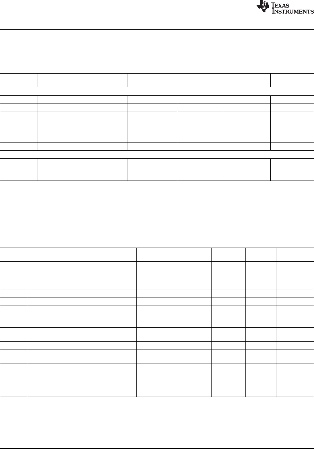
Logic Electrical Characteristics
DIGITAL DC CHARACTERISTICS
Unless otherwise noted, these specifications apply for V
DD
=+3.0 to 3.6 Vdc. Boldface limits apply for T
A
= T
J
= T
MIN
to
T
MAX
; all other limits T
A
= T
J
=+25°C, unless otherwise noted.
Typical
(1)
Limits
(2)
Unit
Symbol Parameter Test Conditions
(Limit)
SMBData, SMBCLK INPUTS
V
IN(1)
Logical “1” Input Voltage 2.1 V (min)
V
IN(0)
Logical “0”Input Voltage 0.8 V (max)
V
IN(HYST)
SMBData and SMBCLK Digital Input 400 mV
Hysteresis
I
IN(1)
Logical “1” Input Current V
IN
= V
DD
0.005 ±10 µA (max)
I
IN(0)
Logical “0” Input Current V
IN
= 0 V −0.005 ±10 µA (max)
C
IN
Input Capacitance 5 pF
ALL DIGITAL OUTPUTS
I
OH
High Level Output Current V
OH
= V
DD
10 µA (max)
V
OL
SMBus Low Level Output Voltage I
OL
= 4mA 0.4 V (max)
I
OL
= 6mA 0.6
(1) Typical values are at T
A
= 25°C and represent most likely parametric norm.
(2) Limits are guaranteed to National's AOQL (Average Outgoing Quality Level).
SMBus DIGITAL SWITCHING CHARACTERISTICS
Unless otherwise noted, these specifications apply for V
DD
=+3.0 Vdc to +3.6 Vdc, C
L
(load capacitance) on output lines = 80
pF. Boldface limits apply for T
A
= T
J
= T
MIN
to T
MAX
; all other limits T
A
= T
J
= +25°C, unless otherwise noted.
The switching characteristics of the LM86 fully meet or exceed the published specifications of the SMBus version 2.0. The
following parameters are the timing relationships between SMBCLK and SMBData signals related to the LM86. They adhere
to but are not necessarily the SMBus bus specifications.
Typical
(1)
Limits
(2)
Unit
Symbol Parameter Test Conditions
(Limit)
f
SMB
SMBus Clock Frequency 100 kHz (max)
10 kHz (min)
t
LOW
SMBus Clock Low Time from V
IN(0)
max to V
IN(0)
max 4.7 µs (min)
25 ms (max)
t
HIGH
SMBus Clock High Time from V
IN(1)
min to V
IN(1)
min 4.0 µs (min)
t
R,SMB
SMBus Rise Time
(3)
1 µs (max)
t
F,SMB
SMBus Fall Time
(4)
0.3 µs (max)
t
OF
Output Fall Time C
L
= 400pF, 250 ns (max)
I
O
= 3mA
(4)
t
TIMEOUT
SMBData and SMBCLK Time Low for Reset of 25 ms (min)
Serial Interface
(5)
35 ms (max)
t
SU;DAT
Data In Setup Time to SMBCLK High 250 ns (min)
t
HD;DAT
Data Out Stable after SMBCLK Low 300 ns (min)
900 ns (max)
t
HD;STA
Start Condition SMBData Low to SMBCLK Low 100 ns (min)
(Start condition hold before the first clock
falling edge)
t
SU;STO
Stop Condition SMBCLK High to SMBData 100 ns (min)
Low (Stop Condition Setup)
(1) Typical values are at T
A
= 25°C and represent most likely parametric norm.
(2) Limits are guaranteed to National's AOQL (Average Outgoing Quality Level).
(3) The output rise time is measured from (V
IN(0)
max + 0.15V) to (V
IN(1)
min − 0.15V).
(4) The output fall time is measured from (V
IN(1)
min - 0.15V) to (V
IN(1)
min + 0.15V).
(5) Holding the SMBData and/or SMBCLK lines Low for a time interval greater than t
TIMEOUT
will reset the LM86's SMBus state machine,
therefore setting SMBData and SMBCLK pins to a high impedance state.
6 Submit Documentation Feedback Copyright © 2001–2013, Texas Instruments Incorporated
Product Folder Links: LM86