
Datasheet


Table Of Contents
- Features
- Applications
- Key Specifications
- Description
- Absolute Maximum Ratings
- Operating Ratings
- Temperature-to-Digital Converter Characteristics
- Logic Electrical Characteristics
- DIGITAL DC CHARACTERISTICS
- SMBus DIGITAL SWITCHING CHARACTERISTICS
- Functional Description
- LM86 REGISTERS
- COMMAND REGISTER
- LOCAL and REMOTE TEMPERATURE REGISTERS (LT, RTHB, RTLB)
- STATUS REGISTER (SR)
- CONFIGURATION REGISTER
- CONVERSION RATE REGISTER
- LOCAL and REMOTE HIGH SETPOINT REGISTERS (LHS, RHSHB, and RHSLB)
- LOCAL and REMOTE LOW SETPOINT REGISTERS (LLS, RLSHB, and RLSLB)
- REMOTE TEMPERATURE OFFSET REGISTERS (RTOHB and RTOLB)
- LOCAL and REMOTE T_CRIT REGISTERS (RCS and LCS)
- T_CRIT HYSTERESIS REGISTER (TH)
- FILTER and ALERT CONFIGURE REGISTER
- MANUFACTURERS ID REGISTER
- DIE REVISION CODE REGISTER
- APPLICATION HINTS
- Data Sheet Revision History
SNP
V+
GND
D1
D2
D4
D3
R1
ESD
Clamp
D5
D6
I/O
LM86
SNIS114E –DECEMBER 2001–REVISED MARCH 2013
www.ti.com
These devices have limited built-in ESD protection. The leads should be shorted together or the device placed in conductive foam
during storage or handling to prevent electrostatic damage to the MOS gates.
Absolute Maximum Ratings
(1)
Supply Voltage −0.3 V to 6.0 V
Voltage at SMBData, SMBCLK, ALERT, T_CRIT_A −0.5V to 6.0V
Voltage at Other Pins −0.3 V to (V
DD
+ 0.3 V)
D− Input Current ±1 mA
Input Current at All Other Pins
(2)
±5 mA
Package Input Current
(2)
30 mA
SMBData, ALERT, T_CRIT_A Output Sink Current 10 mA
Storage Temperature −65°C to +150°C
Soldering Information, Lead Temperature, Vapor Phase (60 seconds) 215°C
SOIC-8 or VSSOP-8 Packages
(3)
Infrared (15 seconds) 220°C
ESD Susceptibility
(4)
Human Body Model 2000 V
Machine Model 200 V
(1) Absolute Maximum Ratings indicate limits beyond which damage to the device may occur. DC and AC electrical specifications do not
apply when operating the device beyond its rated operating conditions.
(2) When the input voltage (V
I
) at any pin exceeds the power supplies (V
I
< GND or V
I
> V
DD
), the current at that pin should be limited to 5
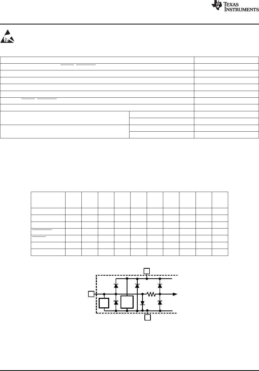
mA. Parasitic components and or ESD protection circuitry are shown in Table 1 and Figure 1 for the LM86's pins. The nominal
breakdown voltage of D3 is 6.5 V. Care should be taken not to forward bias the parasitic diode, D1, present on pins: D+, D−. Doing so
by more than 50 mV may corrupt a temperature measurements.
(3) See the URL ”http://www.national.com/packaging/“ for other recommendations and methods of soldering surface mount devices.
(4) Human body model, 100pF discharged through a 1.5kΩ resistor. Machine model, 200pF discharged directly into each pin.
Table 1. ESD Protection
Pin Name PIN D1 D2 D3 D4 D5 D6 R1 SNP ESD
CLAM
P
V
DD
(V+) 1 x x
D+ 2 x
(1)
x x x x x
D− 3 x x x x x x
T_CRIT_A 4 x x x
ALERT 6 x x x
SMBData 7 x x x
SMBCLK 8 x
(1) An “x” indicates that the diode exists.
Figure 1. ESD Protection Input Structure
4 Submit Documentation Feedback Copyright © 2001–2013, Texas Instruments Incorporated
Product Folder Links: LM86