
Datasheet

LM81
SNAS011E –JUNE 1999–REVISED FEBRUARY 2002
www.ti.com
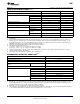
DC ELECTRICAL CHARACTERISTICS
(1)
The following specifications apply for +2.8VDC ≤ V+ ≤ +3.8VDC, RS = 500Ω, unless otherwise specified. Boldface limits
apply for T
A
= T
J
= T
MIN
to T
MAX
; all other limits T
A
= T
J
= 25˚C.
SYMBOL PARAMETER TEST CONDITIONS TYPICAL
(2)
LIMITS LIMITS UNIT
LM81BIM
(3)
LM81CIM
(3)
POWER SUPPLY CHARACTERISTICS
I+ Supply Current Interface Inactive 0.4 1.4 0.9 mA
(max)
TEMPERATURE-TO-DIGITAL CONVERTER CHARACTERISTICS
Error −40˚C ≤ T
A
≤ +125˚C ±3 ±3 ˚C
(max)
Resolution 9-bit mode 0.5 0.5 ˚C
(min)
12-bit mode 0.0625 0.0625 ˚C
(min)
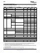
LM81 ANALOG-TO-DIGITAL CONVERTER CHARACTERISTICS
Resolution 8 bits
TUE Total Unadjusted +2.5Vin (See
(4)
and
(5)
) +1.2 +2 %
Error (max)
+3.3Vin −1.2 +0.8 %
(min)
+5Vin
Vccp1, Vccp2 (See
(4)
) +1.2 +2.4 %
(max)
−1.2 0 %
(min)
+12Vin (See
(4)
and
(5)
) +1.2 +3.1 %
(max)
−1.2 +1.2 %
(min)
DNL Differential Non-Linearity ±1 ±1 LSB
(max)
PSS Power Supply Sensitivity ±0.4 %/V
t
C
Total Monitoring Cycle Time (See
(6)
) 0.4 sec
9-bit Temp Resolution 0.82 0.82 sec
(max)
12-bit Temp Resolution 1.2 1.2 sec
(max)
ADC INPUT CHARACTERISTICS
Input Resistance (All analog inputs 115 90 90 kΩ
except Vccp1 and Vccp2) (min)
ADC INPUT CHARACTERISTICS
Vccp1 and Vccp2 DC Input Current ±1 µA
ADC INPUT CHARACTERISTICS
DAC CHARACTERISTICS
Resolution 8 bits
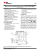
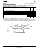
(1) Parasitics and or ESD protection circuitry are shown in the figure below for the LM81’s pins. The nominal breakdown voltage of the
zener D3 is 6.5V. Care should be taken not to forward bias the parasitic diode, D1, present on pins: A0/NTEST_OUT, A1 and
DACOut/NTEST_IN. Doing so by more than 50 mV may corrupt a temperature or voltage measurement.
(2) Typicals are at T
J
= T
A
= 25˚C and represent most likely parametric norm.
(3) Limits are ensured to TI’s AOQL (Average Outgoing Quality Level). Each 9-bit temperature and 8-bit input voltage conversion takes 50
ms typical and 56 ms maximum. Twelve bit temperature conversion takes 400 ms. Fan tachometer readings take 20 ms typical, at 4400
rpm, and 200 ms maximum.
(4) TUE (Total Unadjusted Error) includes Offset, Gain and Linearity errors of the ADC.
(5) Ensured at 3/4 scale ±15%.
(6) Total Monitoring Cycle Time includes temperature conversion, 6 analog input voltage conversions and 2 tachometer readings.
6 Submit Documentation Feedback Copyright © 1999–2002, Texas Instruments Incorporated
Product Folder Links: LM81