
Datasheet
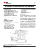
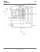

LM81
www.ti.com
SNAS011E –JUNE 1999–REVISED FEBRUARY 2002
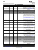
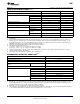
ABSOLUTE MAXIMUM RATINGS
(1)(2)(3)
MIN MAX UNIT
Positive Supply Voltage +6.0 V
Voltage on Any Input or Output Pin: +12Vin, T_CRIT_A -0.3 +15.0 V
A0, A1, DACOut −0.3 (V
+
+ 0.3) V
+2.5Vin, +3.3Vin See
(4)
All other pins −0.3 +6.0 V
Input Current at any Pin
(5)
-5.0 +5.0 mA
Package Input Current
(5)
-20 +20 mA
Maximum Junction Temperature (T
J
max) 150 °C
ESD Susceptibility
(5)
Human Body Model 2000 V
Machine Model 200 V
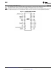
Soldering Information, VSSOP Package
(6)
Vapor Phase (60 215 °C
seconds)
Infrared (15 seconds) 235 °C
Storage Temperature −65 +150 °C
(1) If Military/Aerospace specified devices are required, please contact the Texas Instruments Sales Office/ Distributors for availability and
specifications.
(2) Absolute Maximum Ratings indicate limits beyond which damage to the device may occur. Operating Ratings indicate conditions for
which the device is functional, but do not ensure specific performance limits. For ensured specifications and test conditions, see the
Electrical Characteristics. The ensured specifications apply only for the test conditions listed. Some performance characteristics may
degrade when the device is not operated under the listed test conditions.
(3) All voltages are measured with respect to GND, unless otherwise specified.
(4) The Absolute maximum input range for :
(a) +2.5Vin - −0.3V to (1.4 x V+ + 0.42V or 6V, whichever is smaller
(b) +3.3Vin - −0.3V to (1.8 x V+ + 0.55V or 6V, whichever is smaller.
(5) The human body model is a 100 pF capacitor discharged through a 1.5 kΩ resistor into each pin. The machine model is a 200 pF
capacitor discharged directly into each pin.
(6) See www.ti.com for other methods of soldering surface mount devices.
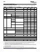
RECOMMENDED OPERATING CONDITIONS
(1)(2)
Operating Temperature Range T
MIN
≤ T
A
≤ T
MAX
LM81 −40°C ≤ T
A
≤ +125°C
Specified Temperature Range T
MIN
≤ T
A
≤ T
MAX
LM81 −40°C ≤ T
A
≤ +125°C
Junction to Ambient Thermal Resistance TI Package Number: PW24A 95°C/W
(θJA
(3)
)
Supply Voltage (V+) +2.8V to +3.8V
V
IN
Voltage Range: +12Vin −0.05V to +15V
+5Vin −0.05V to +6.8V
+3.3Vin −0.05V to +4.6V
+2.5Vin −0.05V to +3.6V
LM84B VID0 - VID4, Vccp, −0.05V to +6.0V
FAN1-FAN2 LM84C VID0 - VID4, Vccp −0.05V to +6.0V
All other inputs −0.05V to (V+ + 0.05V)
(1) Absolute Maximum Ratings indicate limits beyond which damage to the device may occur. Operating Ratings indicate conditions for
which the device is functional, but do not ensure specific performance limits. For ensured specifications and test conditions, see the
Electrical Characteristics. The ensured specifications apply only for the test conditions listed. Some performance characteristics may
degrade when the device is not operated under the listed test conditions.
(2) All voltages are measured with respect to GND, unless otherwise specified.
(3) The maximum power dissipation must be derated at elevated temperatures and is dictated by T
Jmax
, θ
JA
and the ambient temperature,
T
A
. The maximum allowable power dissipation at any temperature is P
D
= (TJ
max
−T
A
)/θ
JA
.
Copyright © 1999–2002, Texas Instruments Incorporated Submit Documentation Feedback 5
Product Folder Links: LM81