
Datasheet
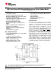

LM81
SNAS011E –JUNE 1999–REVISED FEBRUARY 2002
www.ti.com
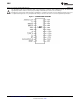
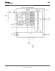
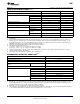
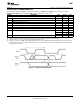
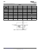
Table 1. PIN DESCRIPTIONS
Pin Name(s) Pin Number Number of Pins Type Description
A0/NTEST_OUT 1 1 Digital I/0 The lowest order programmable bit of the serial
bus address. This pin functions as an output
during NAND Tree tests (board-level connectivity
testing). Refer to the NAND TREE TESTS section.
A1 2 1 Digital Input The highest order programmable bit of the serial
bus address.
SMBData 3 1 Digital I/O Serial Bus bidirectional Data. Open-drain output.
SMBCLK 4 1 Digital Input Serial Bus Clock.
FAN1-FAN2 6-May 2 Digital Inputs Schmitt Trigger fan tachometer inputs.
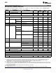
CI 7 1 Digital I/O An active high input from an external circuit which
latches a Chassis Intrusion event. This line can go
high without any clamping action regardless of the
powered state of the LM81. There is also an
internal open-drain output on this line, controlled
by Bit 6 of the Configuration Register (40h) or Bit 7
CI Clear Register (46h), to provide a minimum 20
ms reset pulse. See the USING THE
CONFIGURATION REGISTER and THE LM81
INTERRUPT STRUCTURE sections.
T_CRIT_A 8 1 Digital Output Critical Temperature Alarm active low open-drain
output. This pin can be grounded when not used.
V+ (+2.8V to +3.8V) 9 1 POWER +3.3V V+ power. Bypass with the parallel
combination of 10 µF (electrolytic or tantalum) and
0.1 µF (ceramic) bypass capacitors.
INT 10 1 Digital Output Interrupt active low open-drain output. This output
is enabled when Bit 1 in the Configuration Register
is set to 1. The default state is disabled.
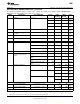
DACOut/NTEST_IN 11 1 Analog Output/Digital 0V to +1.25V amplitude 8-bit DAC output. When
Input forced high by an external voltage the NAND Tree
Test mode is enabled which provides board-level
connectivity testing. Refer to the NAND TREE
TESTS section.
RESET 12 1 Digital I/O Master Reset, 5 mA driver (open-drain), active low
output with a 20 ms minimum pulse width.
Available when enabled via Bit 4 in the
Configuration register. It acts as an active low
power on RESET input.
GND 13 1 GROUND Internally connected to all circuitry. The ground
reference for all analog inputs and the DAC output.
This pin needs to be connected to a low noise
analog ground plane for optimum performance of
the DAC output.
Vccp2 14 1 Analog Input Analog input for monitoring −12V or Vccp2.
Selectable by choosing the appropriate external
resistor divider values such that the input to the
LM81 is scaled to +2.5V. See the ANALOG
INPUTS section.
+12Vin 15 1 Analog Input Analog input for monitoring +12V.
+5Vin 16 1 Analog Input Analog input for monitoring +5V.
+3.3Vin 17 1 Analog Input Analog input for monitoring +3.3V.
+2.5Vin 18 1 Analog Input Analog input for monitoring +2.5V.
Vccp1 19 1 Analog Input Analog input for monitoring Vccp, a processor
voltage that is nominally at +2.5V.
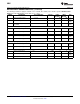
VID4-VID0 20-24 5 Digital Inputs Supply Voltage readouts from the Pentium/PRO
power supplies that indicate the operating voltage
or the processor (e.g. 1.5V to 2.9V). The values
are read in the VID/Fan Divisor Register and the
VID4 Register.
TOTAL PINS 24
4 Submit Documentation Feedback Copyright © 1999–2002, Texas Instruments Incorporated
Product Folder Links: LM81