
Datasheet

LM81
SNAS011E –JUNE 1999–REVISED FEBRUARY 2002
www.ti.com
Thus monitoring power supplies within a system can be easily accomplished by tying the Vccp, +2.5 Vin, +3.3
Vin, +5 Vin and +12 Vin analog inputs to the corresponding system supply. A digital reading can be converted to
a voltage by simply multiplying the decimal value of the reading by the LSB size.
For inputs with attenuators the input impedance is greater than 90 kΩ. Vccp inputs do not have resistor
attenuators and are are directly tied to the ADC, therefore having a much larger input impedance.
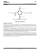
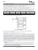
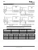
A negative power supply voltage can be applied to a Vccp input through a resistor divider referenced to a known
positive DC voltage as show in Figure 11. The resistor values shown in the table below for the circuit of
Figure 11 will provide approximately 1.25V at the Vccp analog inputs of the LM81 for a nominal reading of 89.
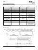
Voltage Measurements R2
(1)
R1
(1)
V+ Voltage at Analog Inputs (ADC code
(VS) 89)
−12V 40 kΩ 141 kΩ +5V +1.25V
−5V 40 kΩ 66.7 kΩ +5V +1.25V
(1) Resistor values shown in table provide approximately 1.25V at the Vccp inputs.
Figure 11. Input Examples
The resistors were selected by setting R2 = 40 kΩ and then calculating R2 using the following equation:
R1 = [(1.25V − VS) ÷ (V+ − 1.25V)] x 40 kΩ (1)
The maximum R1 can be is restricted by the DC input current of a Vccp input.
Inputs with internal resistor dividers (+2.5 Vin, +3.3 Vin or +5 Vin, +12 Vin) can have voltage applied that
exceeds the power supply up to: 3.6V for +2.5 Vin, 4.6V for +3.3 Vin, 6.8V for +5 Vin, and 15V for +12 Vin. The
Vccp inputs have a parasitic diode to the positive supply, so care should be taken not to forward bias this diode.
All analog inputs have internal diodes that clamp the input voltage when going below ground thus limiting the
negative analog input voltage range to −50 mV. Violating the analog input voltage range of any analog input has
no detrimental effect on the other analog inputs. External resistors should be included to limit input currents to
the values given in the ABSOLUTE MAXIMUM RATINGS
(2)(3)(4)
section for Input Current At Any Pin whenever
exceeding the analog input voltage range, even on an un-powered LM81. Inputs with external attenuator
networks will usually meet these requirements. If it is possible for inputs without attenuators (such as Vccp1 and
Vccp2) to be turned on while LM81 is powered off, additional resistors of about 10 kΩ should be added in series
with the inputs to limit the input current.
(2) If Military/Aerospace specified devices are required, please contact the Texas Instruments Sales Office/ Distributors for availability and
specifications.
(3) Absolute Maximum Ratings indicate limits beyond which damage to the device may occur. Operating Ratings indicate conditions for
which the device is functional, but do not ensure specific performance limits. For ensured specifications and test conditions, see the
Electrical Characteristics. The ensured specifications apply only for the test conditions listed. Some performance characteristics may
degrade when the device is not operated under the listed test conditions.
(4) All voltages are measured with respect to GND, unless otherwise specified.
18 Submit Documentation Feedback Copyright © 1999–2002, Texas Instruments Incorporated
Product Folder Links: LM81