
Datasheet

LM81
www.ti.com
SNAS011E –JUNE 1999–REVISED FEBRUARY 2002
STARTING CONVERSIONS
The monitoring function (Analog inputs, temperature, and fan speeds) in the LM81 is started by writing to the
Configuration Register and setting INT_Clear (Bit 3), low, and Start (bit 0), high. The LM81 then performs a
“round-robin” monitoring of all analog inputs, temperature, and fan speed inputs approximately once every 400
ms. The sequence of items being monitored corresponds to locations in the Value RAM and is:
1. Temperature
2. Vccp2
3. +12Vin
4. +5Vin
5. +3.3Vin
6. Vccp1
7. +2.5Vin
8. Fan 1
9. Fan 2
DACOut immediately changes after the DAC Data Register in the Value RAM has been updated. For a zero to
full scale transition DACOut will typically settle within 100 µsec of the stop by master in the write to the DAC Data
Register Serial Bus transaction. The DAC Data Register is not reset by the INITIALIZATION bit found in the
Configuration Register.
READING CONVERSION RESULTS
The conversion results are available in the Value RAM. Conversions can be read at any time and will provide the
result of the last conversion. Because the ADC stops, and starts a new conversion whenever it is read, reads of
any single value should not be done more often than once every 56 ms. When reading all values, allow at least
0.82 seconds between reading groups of values. Reading more frequently than once every 0.82 seconds can
also prevent complete updates of Interrupt Status Registers and Interrupt Outputs.
A typical sequence of events upon power on of the LM81 would consist of:
1. Set WATCHDOG Limits
2. Set Interrupt Masks
3. Start the LM81 monitoring process
DIGITAL COMMUNICATION NOISE CONSIDERATIONS
The SMBData and SMBCLK logic input levels were changed in the SMBus 1.1 specification. SMBus 1.0 levels
were set to 1.4V for a logic high and 0.6V for a logic low. In SMBus 1.1 they were changed to 2.1V for a logic
high and 0.8V for a logic low. Devices that meet the SMBus 1.0 specification have issues in that the logic levels
did not allow for enough noise immunity for some pcb layouts. This has changed with the SMBus 1.1
specification because the higher logic levels allow for more hysteresis in the schmitt trigger inputs stages and
thus more noise immunity. It may be required in some cases to add a series 5.1kΩ resistor connected at the
SMBCLK pin of the LM81C to improve its noise immunity. In addition to meeting the SMBus 1.1 logic levels, the
LM81B has a built-in glitch filter that rejects 100MHz or greater to make it impervious to noise.
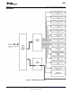
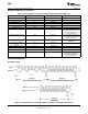
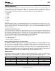
ANALOG INPUTS
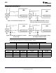
All analog input voltages are digitized to 8-bits of resolution. All analog inputs, except for Vccp1 and Vccp2,
include internal resistor attenuators. The theoretical LSB size, theoretical voltage input required for an ADC
reading of 192 (3/4 scale) and 255 (full scale) for each analog input is detailed in the table below:
Input LSB size Vin for 192 Vin for 255
2.5 Vin 13 mV 2.5V 3.320V
3.3 Vin 17.2 mV 3.3V 4.383V
5 Vin 26 mV 5V 6.641V
12 Vin 62.5 mV 12V 15.93V
Vccp1, Vccp2 14.1 mV 2.7V 3.586V
Copyright © 1999–2002, Texas Instruments Incorporated Submit Documentation Feedback 17
Product Folder Links: LM81