
Datasheet

LM78L05, LM78L09, LM78L12, LM78L15, LM78L62, LM78L82
SNVS754I –JANUARY 2000–REVISED APRIL 2013
www.ti.com
These devices have limited built-in ESD protection. The leads should be shorted together or the device placed in conductive foam
during storage or handling to prevent electrostatic damage to the MOS gates.
DESCRIPTION (CONTINUED)
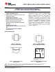
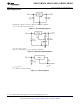
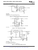
The LM78LXX is available in the plastic TO-92 (LP) package, the SOIC-8 (D) package and a chip sized package
(8-Bump DSBGA) using TI's DSBGA package technology. With adequate heat sinking the regulator can deliver
100mA output current. Current limiting is included to limit the peak output current to a safe value. Safe area
protection for the output transistors is provided to limit internal power dissipation. If internal power dissipation
becomes too high for the heat sinking provided, the thermal shutdown circuit takes over preventing the IC from
overheating.
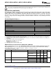
Absolute Maximum Ratings
(1)(2)
Power Dissipation
(3)
Internally Limited
Input Voltage 35V
Storage Temperature −65°C to +150°C
ESD Susceptibility
(4)
1kV
Operating Junction Temperature
LM78LxxACZ, TO-92 0°C to 125°C
LM78LxxACM, SOIC-8 0°C to 125°C
LM78LxxAIM, SOIC-8 -40°C to 125°C
LM78LxxIBPX, DSBGA −40°C to 85°C
LM78LxxITP, Thin DSBGA −40°C to 85°C
Soldering Information
Infrared or Convection (20 sec.) 235°C
Wave Soldering (10 sec.) 260°C (lead time)
(1) Absolute Maximum Ratings indicate limits beyond which damage to the device may occur. Electrical specifications do not apply when
operating the device outside of its stated operating conditions.
(2) If Military/Aerospace specified devices are required, please contact the Texas Instruments Sales Office/Distributors for availability and
specifications.
(3) Typical thermal resistance values for the packages are:
LP Package: θ
JC
= 60 °C/W, = θ
JA
= 230 °C/W
D Package: θ
JA
= 180 °C/W
DSBGA Package: θ
JA
= 230.9°C/W
(4) Human body model, 1.5 kΩ in series with 100pF.
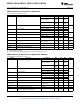
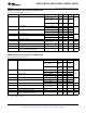
LM78LXX Electrical Characteristics LM78L05AC / LM78L05I
Limits in standard typeface are for T
J
= 25°C, Bold typeface applies over the entire operating temperature range of the
indicated package. Limits are ensured by production testing or correlation techniques using standard Statistical Quality
Control (SQC) methods. Unless otherwise specified: I
O
= 40mA, C
I
= 0.33μF, C
O
= 0.1μF.
Unless otherwise specified, V
IN
= 10V
Symbol Parameter Conditions Min Typ Max Units
V
O
Output Voltage 4.8 5 5.2
7V ≤ V
IN
≤ 20V
1mA ≤ I
O
≤ 40mA 4.75 5.25
V
(1)
1mA ≤ I
O
≤ 70mA
4.75 5.25
(1)
ΔV
O
Line Regulation 7V ≤ V
IN
≤ 20V 18 75
8V ≤ V
IN
≤ 20V 10 54
mV
ΔV
O
Load Regulation 1mA ≤ I
O
≤ 100mA 20 60
1mA ≤ I
O
≤ 40mA 5 30
(1) Power dissipation ≤ 0.75W.
2 Submit Documentation Feedback Copyright © 2000–2013, Texas Instruments Incorporated
Product Folder Links: LM78L05 LM78L09 LM78L12 LM78L15 LM78L62 LM78L82