
Datasheet


LM75B, LM75C
www.ti.com
SNIS153B –JULY 2009–REVISED MARCH 2013
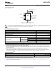
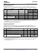
Logic Electrical Characteristics
DIGITAL DC CHARACTERISTICS
Unless otherwise noted, these specifications apply for +V
S
= +5 Vdc for LM75BIM-5, LM75BIMM-5, LM75CIM-5, and
LM75CIMM-5; and +V
S
= +3.3 Vdc for LM75BIM-3, LM75BIMM-3, LM75CIM-3, and LM75CIMM-3
(1)
. Boldface limits apply
for T
A
= T
J
= T
MIN
to T
MAX
; all other limits T
A
= T
J
= +25°C, unless otherwise noted.
Symbol Parameter Conditions Typical
(2)
Limits
(3)
Units (Limit)
+V
S
× 0.7 V (min)
V
IN(1)
Logical “1” Input Voltage
+V
S
+ 0.3 V (max)
−0.3 V (min)
V
IN(0)
Logical “0” Input Voltage
+V
S
× 0.3 V (max)
I
IN(1)
Logical “1” Input Current V
IN
= +V
S
0.005 1.0 μA (max)
I
IN(0)
Logical “0” Input Current V
IN
= 0V −0.005 −1.0 μA (max)
C
IN
All Digital Inputs 5 pF
LM75B V
OH
= 5V 10 μA (max)
I
OH
High Level Output Current
LM75C V
OH
= 5V 100 μA (max)
V
OL
Low Level Output Voltage I
OL
= 3 mA 0.4 V (max)
t
OF
Output Fall Time C
L
= 400 pF I
O
= 3 mA 250 ns (max)
(1) All part numbers of the LM75 will operate properly over the +V
S
supply voltage range of 3V to 5.5V. The devices are tested and
specified for rated accuracy at their nominal supply voltage. Accuracy will typically degrade 1°C/V of variation in +V
S
as it varies from
the nominal value.
(2) Typicals are at T
A
= 25°C and represent most likely parametric norm.
(3) Limits are specified to AOQL (Average Outgoing Quality Level).
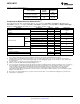
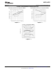
Logic Electrical Characteristics
I
2
C Digital Switching Characteristics
Unless otherwise noted, these specifications apply for V
S
= +5 Vdc for LM75BIM-5, LM75BIMM-5, LM75CIM-5, and
LM75CIMM-5; and +V
S
= +3.3 Vdc for LM75BIM-3, LM75BIMM-3, LM75CIM-3, and LM75CIMM-3C
L
(load capacitance) on
output lines = 80 pF unless otherwise specified. Boldface limits apply for T
A
= T
J
= T
MIN
to T
MAX
; all other limits T
A
= T
J
=
+25°C, unless otherwise noted.
Units
Symbol Parameter Conditions Typical
(1)
Limits
(2)(3)
(Limit)
t
1
SCL (Clock) Period 2.5 μs (min)
t
2
Data in Set-Up Time to SCL High 100 ns (min)
t
3
Data Out Stable after SCL Low 0 ns (min)
t
4
SDA Low Set-Up Time to SCL Low (Start Condition) 100 ns (min)
t
5
SDA High Hold Time after SCL High (Stop Condition) 100 ns (min)
75 ms (min)
LM75B
325 ms (max)
t
TIMEOUT
SDA Time Low for Reset of Serial Interface
(4)
LM75C Not Applicable
(1) Typicals are at T
A
= 25°C and represent most likely parametric norm.
(2) Limits are specified to AOQL (Average Outgoing Quality Level).
(3) Timing specifications are tested at the bus input logic levels (Vin(0)=0.3xVA for a falling edge and Vin(1)=0.7xVA for a rising edge) when
the SCL and SDA edge rates are similar.
(4) Holding the SDA line low for a time greater than t
TIMEOUT
will cause the LM75B to reset SDA to the IDLE state of the serial bus
communication (SDA set High).
Copyright © 2009–2013, Texas Instruments Incorporated Submit Documentation Feedback 5
Product Folder Links: LM75B LM75C