
Datasheet
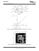


+V
S
A0
A1
A2
SCL
SDA
O.S.
GND
8
7
6
5
3
1
2
4
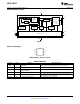
LM75
Address
(Set as desired)
To Processor
Interrupt Line
Interface
100 nF (typ) unless mounted
close to processor
O.S. set to active low
IRUZLUH25¶GPXOWLSOH
interrupt line
LM75B, LM75C
www.ti.com
SNIS153B –JULY 2009–REVISED MARCH 2013
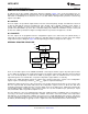
Typical Application
Figure 2. Typical Application
These devices have limited built-in ESD protection. The leads should be shorted together or the device placed in conductive foam
during storage or handling to prevent electrostatic damage to the MOS gates.
Absolute Maximum Ratings
(1)
Supply Voltage Pin (+V
S
) −0.3V to 6.5V
Voltage at A0, A1and A2 Pins −0.3V to (+V
S
+ 0.3V) and must be ≤ 6.5V
Voltage at OS, SCL and SDA Pins −0.3V to 6.5V
Input Current at any Pin
(2)
5 mA
Package Input Current
(2)
20 mA
Storage Temperature −65°C to +150°C
LM75B 2500V
Human Body Model
LM75C 1500V
ESD Susceptibility
(3)
LM75B 250V
Machine Model
LM75C 100V
O.S. Output Sink Current 10 mA
O.S. Output Voltage 6.5V
(1) Absolute Maximum Ratings indicate limits beyond which damage to the device may occur. DC and AC electrical specifications do not
apply when operating the device beyond its rated operating conditions.
(2) When the input voltage (V
I
) at any pin exceeds the power supplies (V
I
< GND or V
I
> +V
S
) the current at that pin should be limited to 5
mA. The 20 mA maximum package input current rating limits the number of pins that can safely exceed the power supplies with an input
current of 5 mA to four.
(3) Human body model, 100 pF discharged through a 1.5 kΩ resistor. Machine model, 200 pF discharged directly into each pin. The
Charged Device Model (CDM) is a specified circuit characterizing an ESD event that occurs when a device acquires charge through
some triboelectric (frictional) or electrostatic induction processes and then abruptly touches a grounded object or surface.
Operating Ratings
(1)(2)
Specified Temperature Range T
MIN
to T
MAX
See
(3)
−55°C to +125°C
Supply Voltage Range (+V
S
) LM75B, LM75C +3.0V to +5.5V
(1) Soldering process must comply with Texas Instruments Incorporated Reflow Temperature Profile specifications. Refer to
(2) Reflow temperature profiles are different for lead-free and non-lead-free packages.
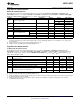
(3) LM75 θ
JA
(thermal resistance, junction-to-ambient) when attached to a printed circuit board with 2 oz. foil similar to the one shown in
Figure 5 is summarized in the table below:
Copyright © 2009–2013, Texas Instruments Incorporated Submit Documentation Feedback 3
Product Folder Links: LM75B LM75C