
Datasheet


LM6171
www.ti.com
SNOS745C –MAY 1998–REVISED MARCH 2013
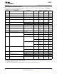
±5V DC Electrical Characteristics
Unless otherwise specified, all limits guaranteed for T
J
= 25°C, V
+
= +5V, V
−
= −5V, V
CM
= 0V, and R
L
= 1 kΩ. Boldface limits
apply at the temperature extremes
Symbol Parameter Conditions Typ LM6171AI LM6171BI Units
(1)
Limit Limit
(2) (2)
V
OS
Input Offset Voltage 1.2 3 6 mV
5 8 max
TC V
OS
Input Offset Voltage Average Drift 4 μV/°C
I
B
Input Bias Current 1 2.5 2.5 μA
3.5 3.5 max
I
OS
Input Offset Current 0.03 1.5 1.5 μA
2.2 2.2 max
R
IN
Input Resistance Common Mode 40 MΩ
Differential Mode 4.9
R
O
Open Loop Output Resistance 14 Ω
CMRR Common Mode Rejection Ratio V
CM
= ±2.5V 105 80 75 dB
75 70 min
PSRR Power Supply Rejection Ratio V
S
= ±15V to ±5V 95 85 80 dB
80 75 min
V
CM
Input Common-Mode Voltage CMRR ≥ 60 dB ±3.7
V
Range
A
V
Large Signal Voltage Gain
(3)
R
L
= 1 kΩ 84 75 75 dB
65 65 min
R
L
= 100Ω 80 70 70 dB
60 60 min
V
O
Output Swing R
L
= 1 kΩ 3.5 3.2 3.2 V
3 3 min
−3.4 −3.2 −3.2 V
−3 −3 max
R
L
= 100Ω 3.2 2.8 2.8 V
2.5 2.5 min
−3.0 −2.8 −2.8 V
−2.5 −2.5 max
Continuous Output Current (Open Sourcing, R
L
= 100Ω 32 28 28 mA
Loop)
(4)
25 25 min
Sinking, R
L
= 100Ω 30 28 28 mA
25 25 max
I
SC
Output Short Circuit Current Sourcing 130 mA
Sinking 100 mA
I
S
Supply Current 2.3 3 3 mA
3.5 3.5 max
(1) Typical Values represent the most likely parametric norm.
(2) All limits are guaranteed by testing or statistical analysis.
(3) Large signal voltage gain is the total output swing divided by the input signal required to produce that swing. For V
S
= ±15V, V
OUT
=
±5V. For V
S
= +5V, V
OUT
= ±1V.
(4) The open loop output current is the output swing with the 100Ω load resistor divided by that resistor.
Copyright © 1998–2013, Texas Instruments Incorporated Submit Documentation Feedback 5
Product Folder Links: LM6171