
Datasheet
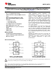
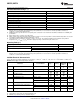
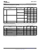
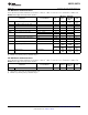
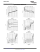
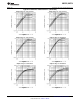
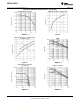
Table Of Contents
- FEATURES
- Applications
- DESCRIPTION
- Absolute Maximum Ratings
- Operating Ratings
- 5.0V DC Electrical Characteristics
- 5.0V AC Electrical Characteristics
- 2.7V DC Electrical Characteristics
- 2.7V AC Electrical Characteristics
- 24V DC Electrical Characteristics
- 24V AC Electrical Characteristics
- Typical Performance Characteristics
- Application Information
- Revision History

LM6152, LM6154
SNOS752D –MAY 1999–REVISED MARCH 2013
www.ti.com
Absolute Maximum Ratings
(1)(2)
ESD Tolerance
(3)
2500V
Differential Input Voltage 15V
Voltage at Input/Output Pin (V
+
) + 0.3V, (V
−
) −0.3V
Supply Voltage (V
+
− V
−
) 35V
Current at Input Pin ±10 mA
Current at Output Pin
(4)
±25 mA
Current at Power Supply Pin 50 mA
Lead Temperature (soldering, 10 sec) 260°C
Storage Temperature Range -65°C to +150°C
Junction Temperature
(5)
150°C
(1) Absolute Maximum Ratings indicate limits beyond which damage to the device may occur. Operating Ratings indicate conditions for
which the device is intended to be functional, but specific performance is not ensured. For ensured specifications and the test
conditions, see the Electrical Characteristics.
(2) If Military/Aerospace specified devices are required, please contact the Texas Instruments Sales Office/ Distributors for availability and
specifications.
(3) Human body model is 1.5 kΩ in series with 100 pF.
(4) Applies to both single-supply and split-supply operation. Continuous short circuit operation at elevated ambient temperature can result in
exceeding the maximum allowed junction temperature of 150°C.
(5) The maximum power dissipation is a function of T
J(MAX)
, θ
JA
, and T
A
. The maximum allowable power dissipation at any ambient
temperature is P
D
= (T
J(MAX)
–T
A
)/θ
JA
. All numbers apply for packages soldered directly into a PC board.
Operating Ratings
(1)
Supply Voltage 2.7V ≤ V
+
≤ 24V
Junction Temperature Range LM6152,LM6154 0°C ≤ T
J
≤ + 70°C
Thermal Resistance (θ
JA
) 8-pin SOIC 193°C/W
14-pin SOIC 126°C/W
(1) Absolute Maximum Ratings indicate limits beyond which damage to the device may occur. Operating Ratings indicate conditions for
which the device is intended to be functional, but specific performance is not ensured. For ensured specifications and the test
conditions, see the Electrical Characteristics.
5.0V DC Electrical Characteristics
Unless otherwise specified, all limits are ensured for T
J
= 25°C, V
+
= 5.0V, V
−
= 0V, V
CM
= V
O
= V
+
/2 and R
L
> 1 MΩ to V
+
/2.
Boldface limits apply at the temperature extremes.
LM6152AC LM6154BC
Parameter Test Conditions Typ
(1)
Limit
(2)
LM6152BC Units
Limit
(2)
V
OS
Input Offset Voltage 0.54 2 5 mV
4 7 max
TCV
OS
Input Offset Voltage Average Drift 10 µV/°C
I
B
Input Bias Current 0V ≤ V
CM
≤ 5V 500 980 980
nA max
750 1500 1500
I
OS
Input Offset Current 32 100 100
nA max
40 160 160
R
IN
Input Resistance, CM 0V ≤ V
CM
≤ 4V 30 MΩ
CMRR Common Mode Rejection Ratio 0V ≤ V
CM
≤ 4V 94 70 70
dB
min
0V ≤ V
CM
≤ 5V 84 60 60
PSRR Power Supply Rejection Ratio 5V ≤ V
+
≤ 24V 91 80 80 dB
min
V
CM
Input Common-Mode Voltage Range Low −0.25 0 0 V
High 5.25 5.0 5.0 V
A
V
Large Signal Voltage Gain R
L
= 10 kΩ 214 50 50 V/mV
min
(1) Typical Values represent the most likely parametric norm.
(2) All limits are specified by testing or statistical analysis.
2 Submit Documentation Feedback Copyright © 1999–2013, Texas Instruments Incorporated
Product Folder Links: LM6152 LM6154