
Datasheet


LM555
SNAS548B –MAY 2004–REVISED JULY 2006
www.ti.com
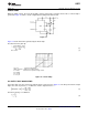
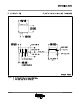
Figure 15. 50% Duty Cycle Oscillator
Note that this circuit will not oscillate if R
B
is greater than 1/2 R
A
because the junction of R
A
and R
B
cannot bring
pin 2 down to 1/3 V
CC
and trigger the lower comparator.
ADDITIONAL INFORMATION
Adequate power supply bypassing is necessary to protect associated circuitry. Minimum recommended is 0.1μF
in parallel with 1μF electrolytic.
Lower comparator storage time can be as long as 10μs when pin 2 is driven fully to ground for triggering. This
limits the monostable pulse width to 10μs minimum.
Delay time reset to output is 0.47μs typical. Minimum reset pulse width must be 0.3μs, typical.
Pin 7 current switches within 30ns of the output (pin 3) voltage.
12 Submit Documentation Feedback Copyright © 2004–2006, Texas Instruments Incorporated
Product Folder Links: LM555