
Datasheet


VDD
P_OUT
N_OUT
VSS
IN
INB
LM5114
PWM
+
VIN
VOUT
VDD
P_OUT
N_OUT
VSS
IN
INB
LM5114
PWM
EN
LM5114
www.ti.com
SNVS790E –JANUARY 2012–REVISED MARCH 2013
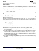
Figure 24. Inverting Application with Enable Pin
Figure 25. A Simplified Boost Converter
Detailed Operating Description
The LM5114 is designed to drive low-side MOSFETs in boost type configurations or to drive secondary
synchronous MOSFETs in isolated topologies. The LM5114 offers both inverting and non-inverting inputs to
satisfy requirements for inverting and non-inverting gate drive in a single device type. Inputs of the LM5114 are
TTL Logic compatible and can withstand the input voltages up to 14V regardless of the VDD voltage. This allows
inputs of the LM5114 to be connected directly to most PWM controllers. The split outputs of the LM5114 offer
flexibility to adjust the turn-on and turn-off speed independently by adding additional impedance in either the turn-
on path and/or the turn-off path.
The LM5114 includes an under-voltage lockout (UVLO) circuit. When the VDD voltage is below the UVLO
threshold voltage, the IN and INB inputs are ignored, and if there is sufficient VDD voltage, the output NMOS is
turned on to pull the N_OUT low. In addition, the LM5114 has an internal PNP transistor in parallel with the
output NMOS. Under the UVLO condition, the PNP transistor will be on and clamp the N_OUT voltage below 1V.
This feature ensures the N_OUT remaining low when VDD voltage is not sufficient to enhance the output NMOS.
The LM5114 has the features necessary to drive low-side enhancement mode GaN FETs. Due to the fast
switching speed and relatively low gate voltage of enhancement mode GaN FETs, PCB layout is crucial to
achieve reliable operation. Refer to Layout Considerations for details.
Copyright © 2012–2013, Texas Instruments Incorporated Submit Documentation Feedback 11
Product Folder Links: LM5114