
Datasheet


LM5109B
SNVS477B –FEBRUARY 2007–REVISED MARCH 2013
www.ti.com
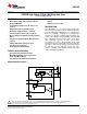
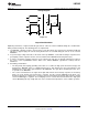
HS Transient Voltages Below Ground
The HS node will always be clamped by the body diode of the lower external FET. In some situations, board
resistances and inductances can cause the HS node to transiently swing several volts below ground. The HS
node can swing below ground provided:
1. HS must always be at a lower potential than HO. Pulling HO more than -0.3V below HS can activate
parasitic transistors resulting in excessive current flow from the HB supply, possibly resulting in damage to
the IC. The same relationship is true with LO and VSS. If necessary, a Schottky diode can be placed
externally between HO and HS or LO and GND to protect the IC from this type of transient. The diode must
be placed as close to the IC pins as possible in order to be effective.
2. HB to HS operating voltage should be 15V or less. Hence, if the HS pin transient voltage is -5V, VDD should
be ideally limited to 10V to keep HB to HS below 15V.
3. Low ESR bypass capacitors from HB to HS and from VDD to VSS are essential for proper operation. The
capacitor should be located at the leads of the IC to minimize series inductance. The peak currents from LO
and HO can be quite large. Any series inductances with the bypass capacitor will cause voltage ringing at the
leads of the IC which must be avoided for reliable operation.
8 Submit Documentation Feedback Copyright © 2007–2013, Texas Instruments Incorporated
Product Folder Links: LM5109B