
Datasheet
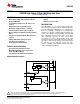


LM5109B
SNVS477B –FEBRUARY 2007–REVISED MARCH 2013
www.ti.com
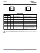
Electrical Characteristics (continued)
Specifications in standard typeface are for T
J
= +25°C, and those in boldface type apply over the full operating junction
temperature range. Unless otherwise specified, V
DD
= V
HB
= 12V, V
SS
= V
HS
= 0V, No Load on LO or HO
(1)
.
Symbol Parameter Conditions Min Typ Max Units
V
HBH
HB Threshold Hysteresis 0.4 V
LO GATE DRIVER
V
OLL
Low-Level Output Voltage I
LO
= 100 mA, V
OHL
= V
LO
– V
SS
0.38 0.65 V
V
OHL
High-Level Output Voltage I
LO
= −100 mA, V
OHL
= V
DD
– V
LO
0.72 1.20 V
I
OHL
Peak Pullup Current V
LO
= 0V 1.0 A
I
OLL
Peak Pulldown Current V
LO
= 12V 1.0 A
HO GATE DRIVER
V
OLH
Low-Level Output Voltage I
HO
= 100 mA, V
OLH
= V
HO
– V
HS
0.38 0.65 V
V
OHH
High-Level Output Voltage I
HO
= −100 mA, V
OHH
= V
HB
– V
HO
0.72 1.20 V
I
OHH
Peak Pullup Current V
HO
= 0V 1.0 A
I
OLH
Peak Pulldown Current V
HO
= 12V 1.0 A
THERMAL RESISTANCE
θ
JA
SOIC-8
(2)(3)
160
Junction to Ambient °C/W
WSON-8
(2)(3)
40
(2) 4 layer board with Cu finished thickness 1.5/1/1/1.5 oz. Maximum die size used. 5x body length of Cu trace on PCB top. 50 x 50mm
ground and power planes embedded in PCB. See the AN-1187 Application Report (SNOA401).
(3) The θ
JA
is not a constant for the package and depends on the printed circuit board design and the operating conditions.
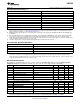
Switching Characteristics
Specifications in standard typeface are for T
J
= +25°C, and those in boldface type apply over the full operating junction
temperature range. Unless otherwise specified, V
DD
= V
HB
= 12V, V
SS
= V
HS
= 0V, No Load on LO or HO.
Symbol Parameter Conditions Min Typ Max Units
t
LPHL
Lower Turn-Off Propagation Delay
30 56 ns
(LI Falling to LO Falling)
t
HPHL
Upper Turn-Off Propagation Delay
30 56 ns
(HI Falling to HO Falling)
t
LPLH
Lower Turn-On Propagation Delay
32 56 ns
(LI Rising to LO Rising)
t
HPLH
Upper Turn-On Propagation Delay
32 56 ns
(HI Rising to HO Rising)
t
MON
Delay Matching: Lower Turn-On and Upper
2 15 ns
Turn-Off
t
MOFF
Delay Matching: Lower Turn-Off and Upper
2 15 ns
Turn-On
t
RC
, t
FC
Either Output Rise/Fall Time C
L
= 1000 pF 15 - ns
t
PW
Minimum Input Pulse Width that Changes
50 ns
the Output
4 Submit Documentation Feedback Copyright © 2007–2013, Texas Instruments Incorporated
Product Folder Links: LM5109B