
Datasheet


LM5109B
www.ti.com
SNVS477B –FEBRUARY 2007–REVISED MARCH 2013
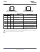
Absolute Maximum Ratings
(1)(2)
V
DD
to V
SS
-0.3V to 18V
HB to HS −0.3V to 18V
LI or HI to V
SS
−0.3V to V
DD
+0.3V
LO to V
SS
−0.3V to V
DD
+0.3V
HO to V
SS
V
HS
−0.3V to V
HB
+0.3V
HS to V
SS
(3)
−5V to 90V
HB to V
SS
108V
Junction Temperature -40°C to +150°C
Storage Temperature Range −55°C to +150°C
ESD Rating HBM
(4)
1.5 kV
(1) Absolute Maximum Ratings indicate limits beyond which damage to the component may occur. Operating Ratings are conditions under
which operation of the device is ensured. Operating Ratings do not imply ensured performance limits. For ensured performance limits
and associated test conditions, see the Electrical Characteristics.
(2) If Military/Aerospace specified devices are required, please contact the Texas Instruments Sales Office/Distributors for availability and
specifications.
(3) In the application the HS node is clamped by the body diode of the external lower N-MOSFET, therefore the HS voltage will generally
not exceed -1V. However in some applications, board resistance and inductance may result in the HS node exceeding this stated
voltage transiently. If negative transients occur on HS, the HS voltage must never be more negative than V
DD
- 15V. For example, if V
DD
= 10V, the negative transients at HS must not exceed -5V.
(4) The human body model is a 100 pF capacitor discharged through a 1.5kΩ resistor into each pin.
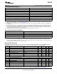
Recommended Operating Conditions
V
DD
8V to 14V
HS
(1)
−1V to 90V
HB V
HS
+8V to V
HS
+14V
HS Slew Rate < 50 V/ns
Junction Temperature −40°C to +125°C
(1) In the application the HS node is clamped by the body diode of the external lower N-MOSFET, therefore the HS voltage will generally
not exceed -1V. However in some applications, board resistance and inductance may result in the HS node exceeding this stated
voltage transiently. If negative transients occur on HS, the HS voltage must never be more negative than V
DD
- 15V. For example, if V
DD
= 10V, the negative transients at HS must not exceed -5V.
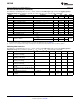
Electrical Characteristics
Specifications in standard typeface are for T
J
= +25°C, and those in boldface type apply over the full operating junction
temperature range. Unless otherwise specified, V
DD
= V
HB
= 12V, V
SS
= V
HS
= 0V, No Load on LO or HO
(1)
.
Symbol Parameter Conditions Min Typ Max Units
SUPPLY CURRENTS
I
DD
V
DD
Quiescent Current LI = HI = 0V 0.3 0.6 mA
I
DDO
V
DD
Operating Current f = 500 kHz 1.8 2.9 mA
I
HB
Total HB Quiescent Current LI = HI = 0V 0.06 0.2 mA
I
HBO
Total HB Operating Current f = 500 kHz 1.4 2.8 mA
I
HBS
HB to V
SS
Current, Quiescent V
HS
= V
HB
= 90V 0.1 10 µA
I
HBSO
HB to V
SS
Current, Operating f = 500 kHz 0.5 mA
INPUT PINS LI and HI
V
IL
Low Level Input Voltage Threshold 0.8 1.8 V
V
IH
High Level Input Voltage Threshold 1.8 2.2 V
R
I
Input Pulldown Resistance 100 200 500 kΩ
UNDER VOLTAGE PROTECTION
V
DDR
V
DD
Rising Threshold V
DDR
= V
DD
- V
SS
6.0 6.7 7.4 V
V
DDH
V
DD
Threshold Hysteresis 0.5 V
V
HBR
HB Rising Threshold V
HBR
= V
HB
- V
HS
5.7 6.6 7.1 V
(1) Min and Max limits are 100% production tested at 25°C. Limits over the operating temperature range are ensured through correlation
using Statistical Quality Control (SQC) methods. Limits are used to calculate Average Outgoing Quality Level (AOQL).
Copyright © 2007–2013, Texas Instruments Incorporated Submit Documentation Feedback 3
Product Folder Links: LM5109B