
Datasheet
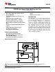
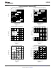


HI
LI
V
SS
HO
HS
LO
HB
V
DD
SOIC-8
1
2
3
4
8
7
6
5
HI
LI
V
SS
HO
HS
LO
HB
V
DD
WSON-8
1
2
3
4
8
7
6
5
LM5109B
SNVS477B –FEBRUARY 2007–REVISED MARCH 2013
www.ti.com
Connection Diagrams
Figure 1. 8-Pin SOIC Package Figure 2. 8-Pin WSON Package
See Package Number D (R-PDSO-G8) See Package Number NGT0008A
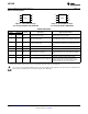
PIN DESCRIPTIONS
Pin #
Name Description Application Information
SOIC-8 WSON-8
(1)
Locally decouple to V
SS
using low ESR/ESL capacitor
1 1 V
DD
Positive gate drive supply
located as close to IC as possible.
The HI input is compatible with TTL input thresholds.
2 2 HI High side control input Unused HI input should be tied to ground and not left
open.
The LI input is compatible with TTL input thresholds.
3 3 LI Low side control input Unused LI input should be tied to ground and not left
open.
4 4 V
SS
Ground reference All signals are referenced to this ground.
5 5 LO Low side gate driver output Connect to the gate of the low-side N-MOS device.
Connect to the negative terminal of the bootstrap
6 6 HS High side source connection capacitor and to the source of the high-side N-MOS
device.
7 7 HO High side gate driver output Connect to the gate of the high-side N-MOS device.
Connect the positive terminal of the bootstrap
capacitor to HB and the negative terminal of the
8 8 HB High side gate driver positive supply rail
bootstrap capacitor to HS. The bootstrap capacitor
should be placed as close to IC as possible.
(1) For WSON-8 package it is recommended that the exposed pad on the bottom of the package be soldered to ground plane on the PCB
and the ground plane should extend out from underneath the package to improve heat dissipation.
These devices have limited built-in ESD protection. The leads should be shorted together or the device placed in conductive foam
during storage or handling to prevent electrostatic damage to the MOS gates.
2 Submit Documentation Feedback Copyright © 2007–2013, Texas Instruments Incorporated
Product Folder Links: LM5109B