
Datasheet


+
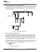
OUTSR
Gate of the Sync
MOSFET needs to be
isolated
3.6V
Secondary Bias Power Good
Secondary Bias
C
BIAS
Q1
Q3
M1
D1
Peak Rectifier
T1
Synchronous Forward MOSFET Enabled
www.ti.com
A diode D1 is connected from the collector to the emitter of Q3 to handle any voltage spikes as a result of
circuit inductance. Without this diode inductive voltage spike may damage the Cascod amplifier Q3.
An NPN transistor was use instead of an N-Channel MOSFET because the Vgs drop, typically 4 to 5 volts;
this would reduce the gates drive voltage to M1. Under minimum input line conditions M1 may not be fully
turned-on and there would be an increase in the I
2
x R
DS(ON)
losses.
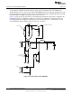
Figure 13 shows the start-up waveforms for the Evaluation board. After the input power is supplied to the
Evaluation board the secondary bias voltage rises, when the secondary bias is greater than 3.6 V, the
Secondary Power Good output goes high. This turns-on M1 and enables the secondary side soft-start
circuit allowing the output voltage to increase after Vout > Vpre-bias.
Figure 12. Isolated Synchronous MOSFET
12
AN-1976 LM5027 Evaluation Board SNVA400B–August 2009–Revised May 2013
Submit Documentation Feedback
Copyright © 2009–2013, Texas Instruments Incorporated