
Datasheet


n
Vin_max
VCE =
16.67 Vpk
6
100
=
=
OUTSR
Gate of the Synchronous
MOSFET needs to be isolated
T1
M1
R2
R1
www.ti.com
Pre-Bias Load-Synchronous Forward MOSFET Enabled
10 Pre-Bias Load-Synchronous Forward MOSFET Enabled
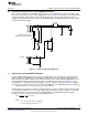
The self driven synchronous rectification topology has an issues starting into a pre-bias load. When a pre-
bias load is connected across the power supply output, refer to Figure 11, the pre-bias source will conduct
current through the output inductor and the self driven gate drive resistors R1 and R2. If the pre-bias
voltage is greater than the Vgs of the synchronous MOSFET (M1), the MOSFET will be turned-on sinking
current into the power supply.
Figure 11. Self Driven with Pre-Bias Load
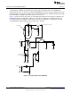
11 Synchronous Forward MOSFET Enabled
For the LM5027 Evaluation board we used the Secondary Bias Power Good signal as a flag to indicate
that the primary sides MOSFETs are switching providing power to the secondary of the transformer T1.
When the flag goes high this indicates that it is time to turn-on the forward conducting MOSFET M1. The
Secondary Bias Power Good signal drives the base of an NPN transistor (Q3), refer to Figure 12. The
NPN transistor is configured as a Cascod amplifier; when it is turned-on, the voltage on the secondary of
the transformer T1 drives the gate of the synchronous MOSFET, M1. The MOSFET gate drive voltage is:
V-GATE_DRIVE_M1 = V_Secondary_Bias_Power_Good-VBE_Q3 (1)
An NPN transistor needs to be selected so that the transistors collector to emitter voltage under the worst
case operating condition does not exceed it’s VCE ratings, and that the collector current (Icc) can handle
the maximum peak current to drive the gate of MOSFET M1. For the LM5027 Evaluation board the
transistor is a 30 V, 1.5 ampere transistor. The maximum VCE is:
where
• Vin = 100 V under transient conditions
• n is the transformer turns ratio = 6
• (2)
11
SNVA400B–August 2009–Revised May 2013 AN-1976 LM5027 Evaluation Board
Submit Documentation Feedback
Copyright © 2009–2013, Texas Instruments Incorporated