
Datasheet


User's Guide
SNVA393B–March 2009–Revised April 2013
AN-1956 LM5001 Boost Evaluation Board
1 Introduction
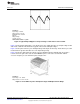
The LM5001 boost evaluation board is designed to provide the design engineer with a fully functional
power converter based on the boost topology to evaluate the LM5001 high voltage switch mode regulator.
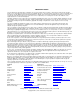
The performance of the evaluation board is as follows:
Input Operating Range: 16 to 36V
Output Voltage: 48V
Output Current: 0 to 150 mA
Measured Efficiency: 91% @ 150 mA, 86% @ 75 mA
Frequency of Operation: 240 kHz
Board Size: 1.75 X 1.75 inches
Load Regulation: 1%
Line Regulation: 0.1%
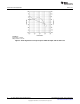
The printed circuit board consists of 2 layers; 1 ounce copper layers FR4 material with a total thickness of
0.062 inches.
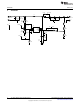
When laying out the PCB note the proximity of the ground pin (pin 4) to the output capacitors (see the
schematic in Section 2). Placing the ground pin near the output capacitor will minimize the ripple in the
output by forcing a constant current to flow across the board for both the switch on and switch off portions
of the cycle. If the board is laid out with the ground pin near the input capacitor then a high di/dt condition
will occur due to the small conduction loop area during the switch on time and large loop conduction area
during the switch off time. The output ripple and noise will be minimized if the conduction loop area and
current both remain constant. Placing the ground pin near the output capacitor accomplishes this goal.
All trademarks are the property of their respective owners.
1
SNVA393B–March 2009–Revised April 2013 AN-1956 LM5001 Boost Evaluation Board
Submit Documentation Feedback
Copyright © 2009–2013, Texas Instruments Incorporated