
Datasheet


Table Of Contents
- Features (LM4121-1.2)
- Applications
- Description
- Absolute Maximum Ratings
- Operating Range
- Electrical Characteristics LM4121-1.250V
- Electrical Characteristics LM4121-ADJ
- LM4121- (All Options) Typical Operating Characteristics
- LM4121-1.25 Typical Operating Characteristics
- LM4121-ADJ Typical Operating Characteristics
- Application Hints
- Revision History
LM4121
www.ti.com
SNVS073C –APRIL 2000–REVISED APRIL 2013
Operating Range
(1)
Storage Temperature Range −65°C to +150°C
Ambient Temperature Range −40°C to +85°C
Junction Temperature Range −40°C to +125°C
(1) “Absolute Maximum Ratings” indicate limits beyond which damage to the device may occur. Operating Ratings indicate conditions for
which the device is intended to be functional, but do not ensure specific performance limits. For ensured specifications and test
conditions, see Electrical Characteristics - LM4121-1.250V and Electrical Characteristics - LM4121-ADJ tables. The ensured
specifications apply only for the test conditions listed. Some performance characteristics may degrade when the device is not operated
under the listed test conditions.
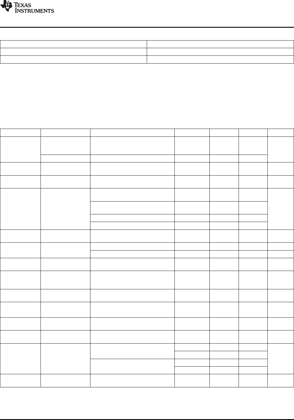
Electrical Characteristics
LM4121-1.250V
Unless otherwise specified V
IN
= 3.3V, I
LOAD
= 0, C
OUT
= 0.01µF, T
A
= T
j
= 25°C. Limits with standard typeface are for T
j
=
25°C, and limits in boldface type apply over the −40°C ≤ T
A
≤ +85°C temperature range.
Symbol Parameter Conditions Min
(1)
Typ
(2)
Max
(1)
Units
V
OUT
Output Voltage Initial
Accuracy 1.250 ±0.2
%
LM4121A-1.250
LM4121-1.250 ±0.5
TCV
OUT
/°C Temperature −40°C ≤ T
A
≤ +125°C 14 50 ppm/°c
Coefficient
ΔV
OUT
/ΔV
IN
Line Regulation 1.8V ≤ V
IN
≤ 12V 0.0007 0.009
%/V
0.012
0 mA ≤ I
LOAD
≤ 1 mA 0.03 0.08
0.17
1 mA ≤ I
LOAD
≤ 5 mA 0.01 0.04
ΔV
OUT
/ΔI
LOAD
Load Regulation %/mA
0.1
−1 mA ≤ I
LOAD
≤ 0 mA 0.04 0.12
−5 mA ≤ I
LOAD
≤ −1 mA 0.01
Min-V
IN
Minimum Operating I
LOAD
= 5mA 1.5 1.8 V
Voltage
V
N
Output Noise Voltage 0.1 Hz to 10 Hz 20 µV
PP
10 Hz to 10 kHz 30 µV
RMS
I
S
Supply Current 160 250 µA
275
I
SS
Power-down Supply V
IN
= 12V
Current Enable = 0.4V 1 µA
Enable = 0.2V 2
V
H
Logic High Input 1.6 1.5 V
Voltage
V
L
Logic Low Input 0.4 V
Voltage
0.2
I
H
Logic High Input 7 15 µA
Current
I
L
Logic Low Input 0.1 µA
Current
V
IN
= 3.3V, V
OUT
= 0 15
6 30
I
SC
Short Circuit Current mA
V
IN
= 12V, V
OUT
= 0 17
6 30
Hyst Thermal Hysteresis −40°C ≤ T
A
≤ 125°C 0.5 mV/V
(3)
(1) Limits are 100% production tested at 25°C. Limits over the operating temperature range are ensured through correlation using Statistical
Quality Control (SQC) methods. The limits are used to calculate TI's Averaging Outgoing Quality Level (AOQL).
(2) Typical numbers are at 25°C and represent the most likely parametric norm.
(3) Thermal hysteresis is defined as the change in +25°C output voltage before and after exposing the device to temperature extremes.
Copyright © 2000–2013, Texas Instruments Incorporated Submit Documentation Feedback 3
Product Folder Links: LM4121