
Datasheet


Table Of Contents
- Features (LM4121-1.2)
- Applications
- Description
- Absolute Maximum Ratings
- Operating Range
- Electrical Characteristics LM4121-1.250V
- Electrical Characteristics LM4121-ADJ
- LM4121- (All Options) Typical Operating Characteristics
- LM4121-1.25 Typical Operating Characteristics
- LM4121-ADJ Typical Operating Characteristics
- Application Hints
- Revision History
(+)
(-)
I =
1.216
R
R
I
EN
ADJ
GND
V
OUT
LM4121-ADJ
0.022PF
V
IN
V
IN
R
1
EN
V
IN
V
OUT
2N3904
R
2
+
V
O
2.2PF
GND
ADJ
LM4121-ADJ
0.022PF
V
O
= 1.216 (
R
1
+ 1)
R
2
LM4121
www.ti.com
SNVS073C –APRIL 2000–REVISED APRIL 2013
PRINTED CIRCUIT BOARD LAYOUT CONSIDERATION
The mechanical stress due to PC board mounting can cause the output voltage to shift from its initial value.
References in SOT packages are generally less prone to assembly stress than devices in Small Outline (SOIC)
package.
To reduce the stress-related output voltage shifts, mount the reference on the low flex areas of the PC board
such as near to the edge or the corner of the PC board.
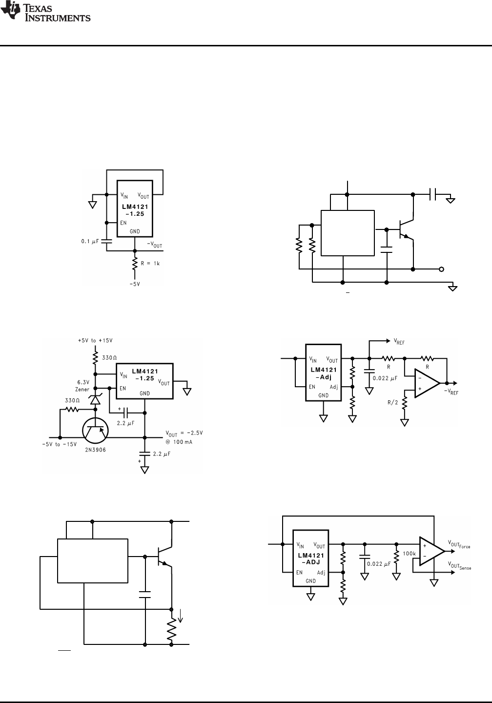
Typical Application Circuits
Figure 35. Voltage Reference with Negative Output Figure 36. 100mA Quasi-LDO Regulator
Figure 37. Boosted Output Current with Figure 38. Voltage Reference with Complimentary
Output
Negative Voltage Reference
Figure 39. Two Terminal Constant Current Source Figure 40. Precision Voltage Reference
with Force and Sense Output
Copyright © 2000–2013, Texas Instruments Incorporated Submit Documentation Feedback 13
Product Folder Links: LM4121