
Datasheet


Table Of Contents
PCB Layout
www.ti.com
9 PCB Layout
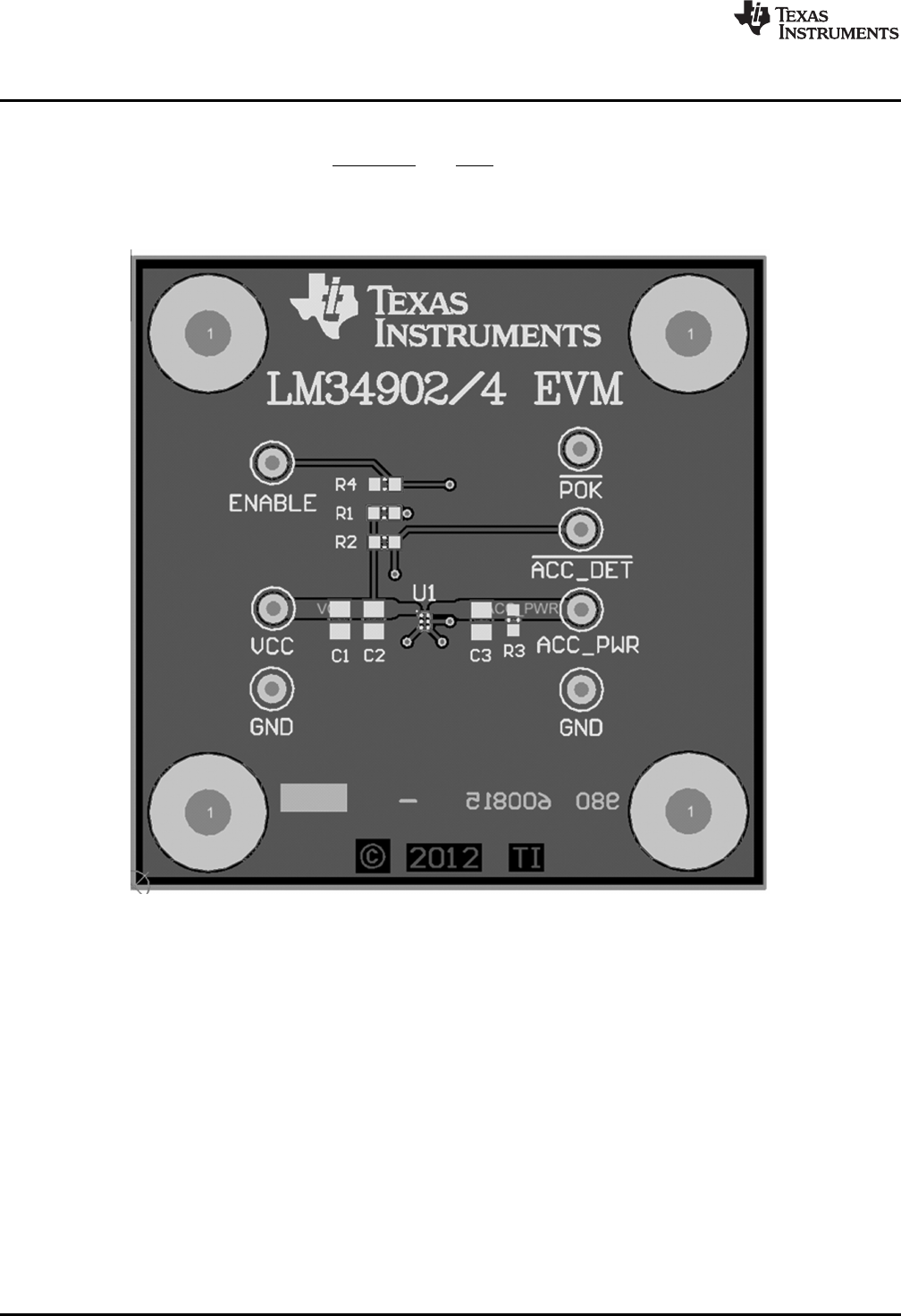
The LM34902/4 evaluation module uses a two-layer FR4 PCB with terminal connections provided for
VCC, ACC_PWR, GND, ENABLE, ACC_DET and POK. The top and bottom side PCB layouts are shown
in Figure 10 and Figure 11, respectively.
Figure 10. PCB Top Layer
6
AN-2266 LM34902/4 Current Limited Power Switch Evaluation Module SNVU156A–July 2012–Revised May 2013
Submit Documentation Feedback
Copyright © 2012–2013, Texas Instruments Incorporated