
User manual
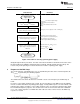
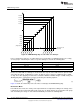

LM3463 EVALUATION BOARD
WARNING:
HIGH DC VOLTAGE
J0
J1
J11
J12
J13
J14
J15
J16
J2
J9J5J7
J4J6J8
J10
J3
CH0 CH1 CH2 CH3 CH4 CH5VRAIL
GND
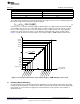
LM3463 EVALUATION BOARD
WARNING:
HIGH DC VOLTAGE
J0
J1
J11
J12
J13
J14
J15
J16
J2
J9J5J7
J4J6J8
J10
J3
CH0 CH1 CH2 CH3 CH4 CH5VRAIL
GND
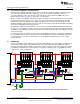
LM3463 EVALUATION BOARD
WARNING:
HIGH DC VOLTAGE
J0
J1
J11
J12
J13
J14
J15
J16
J2
J9J5J7
J4J6J8
J10
J3
CH0 CH1 CH2 CH3 CH4 CH5VRAIL
GND
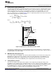
TP12
TP14
TP33
TP35
VFB
TP12
TP14
TP33
TP35
VFB
J4 = OPEN J7 = SHORT 2-3
J5 = OPEN J8 = OPEN
J6 = OPEN J9 = OPEN
TP22
TP3
TP22
TP3
TP22
TP3
MASTER
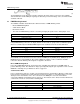
J4 = OPEN J7 = SHORT 2-3
J5 = OPEN J8 = OPEN
J6 = SHORT 2-3 J9 = OPEN
VLedFB = VCC
R2 = OPEN
R4 = OPEN
SLAVE 1
J4 = OPEN J7 = SHORT 2-3
J5 = OPEN J8 = OPEN
J6 = SHORT 2-3 J9 = OPEN
VLedFB = VCC
R2 = OPEN
R4 = OPEN
SLAVE 2
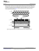
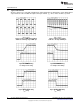
LED array 1 LED array 2 LED array 3VRAIL
GND
VFB
Primary Power Supply
TP12
TP14
TP16
LOAD
SCLK
SDAT
Interface to MCU for
dimming control
Cascading the LM3463 evaluation board
www.ti.com
14 Cascading the LM3463 evaluation board
A number of the LM3463 evaluation boards can be cascaded to expand the number of output channels.
The connection among boards differs depending on the selected mode for dimming control. The
connection diagrams for the serial interface mode, DC interface mode and direct PWM mode are as
illustrated in the Figure 12, Figure 13, and Figure 14, respectively.
When a number of the LM3463 evaluation boards are cascaded, one of the boards must be set as master
unit and the other boards must be set as slave units. The master unit is the board which has the VFB
terminal connected to the primary power supply. The master unit controls the system startup time and
distributes dimming control signals to the slave units, the connections among the boards differs depending
on the mode of dimming control being selected.
By default, the LM3463 evaluation board is set as a master unit in direct PWM dimming mode with 100%
on duty. To set a board to be a slave unit, the resistors R2 and R4 must be removed and the terminal TP3
(VLedFB pin of the LM3463) should be connected to the terminal TP22 (VCC pin of the LM3463) using an
external connection.
In cascade operation, the number of slave units is virtually unlimited. However, in high power applications
the accumulated voltage drop on the power return part could impair the function of the DHC. Generally it
is suggested not to cascade more than four pieces of the LM3463 evaluation board to secure stable
system operation.
15 PCB Design
Good heat dissipation helps optimize the performance of the LM3463. The ground plane should be used
to connect the exposed pad of the LM3463, which is internally connected to the LM3463 die substrate.
The area of the ground plane should be extended as much as possible on the same copper layer around
the LM3463. Using numerous vias beneath the exposed pad to dissipate heat of the LM3463 to another
copper layer is also a good practice.
Figure 12. A 12 channel lighting system using serial interface mode for dimming control
14
AN-2255 LM3463 Evaluation Board SNVA642A–May 2012–Revised May 2013
Submit Documentation Feedback
Copyright © 2012–2013, Texas Instruments Incorporated