
User manual

Analog voltage
at the DIMn pin
2/256
PWM dimming duty
3/256
4/256
0
5/256
5
.
7
V-V
LSB
5
.
7
V-2
V
LSB
5
.
7
V
5
.
7
V
-
3
V
LSB
256/256
5
.
7
V-4
V
LSB
255/256
254/256
253/256
252/256
0
.
8
V
+
3
V
LSB
0
.
8
V
+
2
V
LSB
0
.
8
V
+
4
V
LSB
0
.
8
V
+
V
LSB
0
.
8
V
6/256
V
LSB
=
5.7V - 0.8V
256
(Skipped) 1/256
www.ti.com
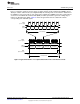
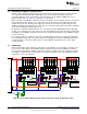
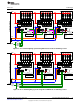
Disabling Output Channel(s)
Output channel Terminal
CH0, CH1 TP12
CH2, CH3 TP14
CH4 TP16
CH5 TP18
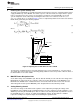
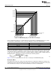
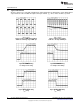
The voltage being applied to the terminals should be in the range of 0.8V to 5.7V. The dimming duty in the
DC interface mode is governed by the following equation:
(6)
In this mode, the conversion of analog voltage to dimming duty is accomplished by an internal 8-bit ADC
of the LM3463, thus the step size of the LED current is equal to 1/256 of the full scale current. To allow
the use of 0% on duty, the steps 1 and 2 are combined to give a 2/256 on duty. Thus either applying a
voltage in the range of 0.8V to 0.8V+V
LSB
to the dimming control inputs will result in a 2/256 on duty.
Figure 11 shows the Conversion characteristics of the analog voltage to PWM dimming control circuit:
Figure 11. Conversion characteristic of the analog voltage to PWM dimming control circuit
13 Disabling Output Channel(s)
An output channel of this evaluation board can be disabled by not connecting an LED string to the output
terminal. A disabled channel is excluded from the DHC loop and remained in OFF state until a falling edge
at the EN pin or system repower is applied. The channel 0 must be used regardless of the number of
disabled channel.
13
SNVA642A–May 2012–Revised May 2013 AN-2255 LM3463 Evaluation Board
Submit Documentation Feedback
Copyright © 2012–2013, Texas Instruments Incorporated