
User manual
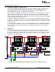

BIT7BIT6BIT5BIT4BIT3BIT2BIT1BIT0
One data byte
DIM01
DIM23
(Clock signal)
(Data)
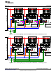
DIM01
DIM23
(Clock signal)
(Data)
BYTE1
(Group D)
BYTE2
(Group C)
BYTE3
(Group B)
BYTE4
(Group A)
DIM4
(End of Frame)
EOF
One data frame
LSB MSB
BOF
www.ti.com
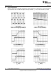
PWM Dimming Control
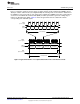
In the serial interface mode the LM3463 evaluation board accepts a data frame which consists of four data
bytes to control the on duty of the four groups of output channels via the terminal TP12 (DIM01). Every
data byte contains 8 bits in LSB (Least Significant Bit) first ordering and is clocked into the data buffer of
the LM3463 at every rising edge of clock signal at the terminal TP14 (DIM23). Every time a data frame is
clocked in to the LM3463 the terminal TP16 (DIM4) should be pulled low to generate a falling edge to
indicate an ‘End-Of-Frame (EOF)’. Figure 9 shows the typical waveform of a data frame and the
corresponding clock and EOF signals.
Figure 9. Typical waveforms of a complete data frame in the serial interface mode
11
SNVA642A–May 2012–Revised May 2013 AN-2255 LM3463 Evaluation Board
Submit Documentation Feedback
Copyright © 2012–2013, Texas Instruments Incorporated