
User manual

PWM Dimming Control
www.ti.com
(4)
The IOUTADJ pin can be biased by a positive voltage in the range of 0V to 2.5V across the terminals
TP31and TP39. If the IOUTADJ pin is going to be biased by an external voltage source, the R10 and R11
should be removed.
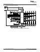
12 PWM Dimming Control
The LM3463 evaluation board allows three different modes of PWM dimming control:
• Direct PWM Dimming Mode
• Serial Interface Mode
• DC Interface Mode
• The mode of PWM dimming control is selected by changing the position of the shunt jumper of J8.
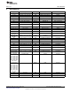
Mode of dimming control Setting of J8
Direct PWM dimming mode Short Pos. 2–3
Serial interface mode Open
DC interface mode Short Pos. 1–2
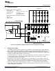
Using PWM dimming control, the six output channels of the board are grouped into four individual groups
which are controlled by four individual PWM signals at the terminals TP12, TP14, TP16 and TP18.
Terminal Involved channels
TP12 CH0, CH1
TP14 CH2, CH3
TP16 CH4
TP18 CH5
The terminals J4, J5, J6 and J7 are used to connect the DIM01(TP12), DIM23(TP14), DIM4(TP16) and
DIM5(TP18) pins of the LM3463 to either VCC or GND. The jumpers on these terminals should be
removed if external dimming control signals are applied to the board.
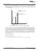
Direct PWM Dimming Mode
In the direct PWM dimming mode, the board accepts standard active high TTL level PWM signals to
perform dimming control. The minimum on duty is generally limited by the gate capacitance of the external
MOSFETs. Normally, an 8 µs minimum on time is suggested.
Serial Interface Mode
In the serial interface mode, the on duty of each output channel is controlled by a data byte of 8 bits wide.
In this mode the terminals TP12, TP14 and TP16 on the board comprise a serial data interface to receive
data bytes from external data source. The connection to the DIM5 pin is not used and should be
connected to GND by shortening the pins 2 and 3 of J7. The functions of the TP12, TP14 and TP16 in the
serial interface mode are as listed in the following table:
Serial Interface Mode
Terminal Function
TP12 Serial data input
TP14 Clock signal input
TP16 End Of data Frame (EOF) signal input
10
AN-2255 LM3463 Evaluation Board SNVA642A–May 2012–Revised May 2013
Submit Documentation Feedback
Copyright © 2012–2013, Texas Instruments Incorporated