
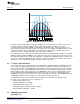
User manual
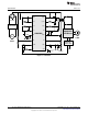
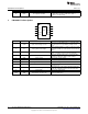
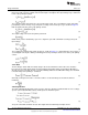

UVLO
1
CSP
2
VIN
3
4
8
COFF
7
EN
6
CSN
5
9
10
GND PGATE
DAP
VCC
IADJ
LM3409HV Pin Descriptions
www.ti.com
Pin Name Description Application Information
Pre-regulator Gate Bias Output: Connect to gate of
16 BIAS Pre-regulator Gate Bias passFET and to resistor to rectified AC (drain of
passFET) to aid with startup.
7 LM3409HV Pin Descriptions
Pin Name Description Application Information
Connect to a resistor divider from V
IN
. UVLO threshold is
1 UVLO Input Under Voltage Lock-out 1.24V and hysteresis is provided by a 22µA current
source.
Apply a voltage between 0 - 1.24V, or connect a resistor
2 I
ADJ
Analog LED Current Adjust from this pin to GND, to set the current sense threshold
voltage.
Apply a voltage >1.6V to enable device, a PWM signal
3 EN Logic Level Enable
to dim, or a voltage <0.6V for low power shutdown.
Connect an external resistor from V
O
to this pin, and a
4 COFF Off-time programming
capacitor from this pin to GND to set the off-time.
5 GND Power Ground Connect to the system ground.
6 PGATE Gate Drive Connect to the gate of the external PFET.
7 CSN Negative Current Sense Connect to the negative side of the sense resistor.
Connect to the positive side of the sense resistor (also
8 CSP Positive Current Sense
connected to V
IN
).
Connect at least a 1 µF ceramic capacitor from this pin
9 V
CC
V
IN
-referenced Linear Regulator Output
to CSN. The regulator provides power for P-FET drive.
10 V
IN
Input Voltage Connect to the input voltage.
Connect to pin 5 (GND). Place 4-6 vias from DAP to
DAP DAP Thermal PAD on bottom of IC
bottom layer GND plane.
6
AN-2150 LM3450A Evaluation Board SNVA485B–June 2011–Revised May 2013
Submit Documentation Feedback
Copyright © 2011–2013, Texas Instruments Incorporated