
User manual
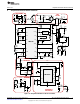

V
CC
V
REF
ZCDFLT2
DIM GATE
V
AC
CS
COMP GND
FB I
SEN
HOLDV
ADJ
FLT1
BIAS
9
10
11
12
13
14
15
16
8
7
6
5
4
3
2
1
www.ti.com
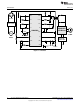
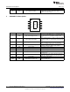
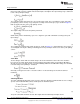
LM3450A Pin Descriptions
6 LM3450A Pin Descriptions
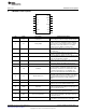
Pin Name Description Application Information
Reference Output: Connect directly to V
ADJ
or to resistor
1 V
REF
3V Reference
divider feeding V
ADJ
and to necessary external circuits.
Analog Dim and Phase Dimming Range Input: Connect
directly to V
REF
to force standard 70% phase dimming
2 V
ADJ
Analog Adjust range. Connect to resistor divider from V
REF
to extend
usable range of some phase dimmers or for analog
dimming. Connect to GND for low power mode.
Ramp Comparator Input: Connect a series resistor from
3 FLT2 Filter 2 FLT1 capacitor and a capacitor to GND to establish
second filter pole.
Angle Decoder Output: Connect a series resistor to a
4 FLT1 Filter 1
capacitor to ground to establish first filter pole.
Open Drain PWM Dim Output: Connect to dimming input
5 DIM 500 Hz PWM Output of output stage LED driver (directly or with isolation) to
provide decoded dimming command.
Multiplier and Angle Decoder Input: Connect to resistor
6 V
AC
Sampled Rectified Line
divider from rectified AC line.
Error Amplifier Output and PWM Comparator Input:
7 COMP Compensation
Connect a capacitor to GND to set the compensation.
Error Amplifier Inverting Input: Connect to output voltage
via resistor divider to control PFC voltage loop for non-
8 FB Feedback isolated designs. Connect to a 5.11kΩ resistor to GND
for isolated designs (bypasses error amplifier). Also
includes over-voltage protection and shutdown modes.
Input Current Sense Non-Inverting Input: Connect to
diode bridge return and resistor to GND to sense input
9 I
SEN
Input Current Sense current for dynamic hold. Connect a 0.1µF capacitor and
Schottky diode to GND, and a 0.22µF capacitor to
HOLD.
10 GND Power Ground System Ground
MosFET Current Sense Input: Connect to positive
11 CS Current Sense
terminal of sense resistor in PFC MosFET source.
Gate Drive Output: Connect to gate of main power
12 GATE Gate Drive MosFET for PFC.Gate Drive Output: Connect to gate of
main power MosFET for PFC.
Power Supply Input: Connect to primary bias supply.
13 V
CC
Input Supply
Connect a 0.1µF bypass capacitor to ground.
Demagnetization Sense Input: Connect a resistor to
14 ZCD Zero Crossing Detector transformer/inductor winding to detect when all energy
has been transferred.
Open Drain Dynamic Hold Input: Connect to holding
15 HOLD Dynamic Hold
resistor which is connected to source of passFET.
5
SNVA485B–June 2011–Revised May 2013 AN-2150 LM3450A Evaluation Board
Submit Documentation Feedback
Copyright © 2011–2013, Texas Instruments Incorporated