
User manual

0.0 0.2 0.4 0.6 0.8 1.0
0.0
0.2
0.4
0.6
0.8
1.0
1.2
LM3409HV EN PIN DUTY CYCLE
LM3450A DEMODULATED VAC PIN DUTY CYCLE
1V
0.5V
2V
2.5V
1.5V
V
ADJ
=3V
Design Information
www.ti.com
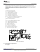
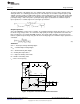
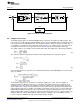
Decoder Mapping
The mapping from the demodulated input (VAC pin of the LM3450A) to output (EN pin of the LM3409HV)
is shown in Figure 17. Varying V
ADJ
will adjust the mapping as desired for the target dimmers. Keep in
mind that the demodulated input angle is a function of the resistor divider at the V
AC
pin. This means that
the input duty cycle can be shifted by changing V
DET
within the previously suggested range.
Filters
The filters (FLT1, FLT2) are chosen to provide the desired dimming transition response (how the light
changes during dimmer movement). The filter frequency should be set between 2Hz and 10Hz for best
operation (2Hz has a fade feeling, 10Hz is very snappy). The capacitors (C17, C18) can both be set to
1µF for all designs and given the filter frequencies, the resistors (R24, R25) are calculated:
(24)
Figure 17. Dimming Decoder Mapping
Opto-Isolator
A standard low cost opto-isolator (same type used for feedback of the output) is used to transfer the
dimming command from DIM to the secondary. It needs to be driven with at least 1-2mA of current to
obtain full 70:1 contrast ratio (more current creates faster edges). With V
POP2
= 9V and R16 = 6.04kΩ,
there is > 1mA of drive current. The output of the opto-isolator should be clamped to just above the
dimming input threshold of the secondary driver. This is accomplished with a 1.8V Zener clamp (D22) at
the EN pin of the LM3409HV on the evaluation boards. R71 needs to be large enough that the Zener
clamp is activated whenever the LM3409HV EN pin should be high.
Definitions
V
DET
– Rectified AC Angle Detect Voltage
f
FLT1
– FLT1 frequency
f
FLT2
– FLT2 frequency
18
AN-2150 LM3450A Evaluation Board SNVA485B–June 2011–Revised May 2013
Submit Documentation Feedback
Copyright © 2011–2013, Texas Instruments Incorporated