
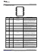
User manual

Design Information
www.ti.com
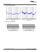
The AC mains voltage, at the line frequency f
L
, is assumed to be perfectly sinusoidal and the diode bridge
ideal. This yields a perfect rectified sinusoid at the input to the flyback. The input voltage V
in
(t) is defined in
terms of the peak input voltage:
(1)
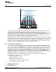
The controller and the transformer are also assumed to be ideal. These assumptions yield a sinusoidal
peak primary current envelope I
P-pk
(t) and peak secondary current envelope I
S-pk
(t) as shown in Figure 12.
Both are defined in terms of the peak primary current:
(2)
The output voltage reflected to the primary is defined:
(3)
CRM control yields a variable duty cycle over a single line cycle with a minimum occurring at the peak
input voltage:
(4)
The resulting sinusoidal average input current I
in
(t), shown in Figure 12, is approximated as the average of
each triangular current pulse during a switching period. The peak input current occurs at the peak primary
current:
(5)
Turns Ratio
The first thing to decide with an isolated design is the desired transformer turns ratio. This should be
based on the specified output voltage and the maximum peak input voltage. Frequently the MosFET is
already chosen for a design, given its cost and availability. With a desired MosFET voltage, the maximum
reflected voltage at the primary is calculated:
(6)
Generally, an integer turns ratio is selected to achieve a reflected voltage at or below the defined
maximum:
(7)
Switching MosFET
The main switching MosFET (Q3) can be sized as desired; to block the maximum drain-to-source voltage,
operate at the maximum RMS current, and dissipate the maximum power:
(8)
The peak current limit should be at least 25% higher than the maximum peak input current:
10
AN-2150 LM3450A Evaluation Board SNVA485B–June 2011–Revised May 2013
Submit Documentation Feedback
Copyright © 2011–2013, Texas Instruments Incorporated