User's Guide SNVA485B – June 2011 – Revised May 2013 AN-2150 LM3450A Evaluation Board 1 Introduction The LM3450A evaluation board is designed to provide an AC to LED solution for a 30W LED load. Specifically, it takes an AC mains input and converts it to a constant current output of 700mA for a series string of 1 to 13 LEDs (maximum LED stack voltage of 45V). There are two assembly versions designed to operate from two different nominal AC input voltages, 120VAC or 230VAC. .
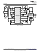
Specifications www.ti.com VREF BIAS VADJ HOLD RETURN EMI FILTER FLT2 ZCD FLT1 VCC LM3409HV LED Driver LM3450A PWM AC INPUT DIM VAC COMP FB GATE LED LOAD CS OPTICAL ISOLATION GND ISEN PWM HOLD RETURN Figure 1.
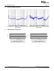
Typical Performance www.ti.com 3 Typical Performance 84 84 82 120 VAC EFFICIENCY (%) EFFICIENCY (%) 82 80 100 VAC 78 76 16 200 VAC 230 VAC 80 78 20 24 28 76 16 32 20 24 28 32 POUT (W) POUT (W) Figure 2. 120V, 30W Version Efficiency vs. Output Power Figure 3. 230V, 30W Version Efficiency vs. Output Power 1.00 1.00 100 VAC 0.98 200 VAC 0.98 PF PF 120 VAC 0.96 0.94 0.92 16 0.96 230 VAC 0.94 20 24 28 32 0.92 16 20 POUT (W) Figure 4.
Conducted EMI Performance Conducted EMI Performance AMPLITUDE in dbuV AMPLITUDE in dbuV 4 www.ti.com FREQUENCY FREQUENCY Figure 6. 120V, 30W Conducted EMI Peak Scan Figure 7.
LM3450A Pin Descriptions www.ti.com 6 LM3450A Pin Descriptions 1 2 3 4 5 6 7 8 Pin 1 Name VREF VREF BIAS VADJ HOLD FLT2 ZCD FLT1 VCC DIM GATE VAC CS COMP FB GND ISEN 16 15 14 13 12 11 10 9 Description Application Information 3V Reference Reference Output: Connect directly to VADJ or to resistor divider feeding VADJ and to necessary external circuits. 2 VADJ Analog Adjust Analog Dim and Phase Dimming Range Input: Connect directly to VREF to force standard 70% phase dimming range.
LM3409HV Pin Descriptions 7 www.ti.com Pin Name Description 16 BIAS Pre-regulator Gate Bias Pre-regulator Gate Bias Output: Connect to gate of passFET and to resistor to rectified AC (drain of passFET) to aid with startup. LM3409HV Pin Descriptions 1 2 3 4 5 Pin 6 Application Information Name UVLO VIN IADJ VCC EN DAP CSP COFF GND CSN PGATE 10 9 8 7 6 Description Application Information 1 UVLO Input Under Voltage Lock-out Connect to a resistor divider from VIN.
Simplified Evaluation Board Schematic www.ti.
Design Information 9 www.ti.com Design Information The following section explains how to design using the LM3450A power factor controller and phase dimming decoder. Refer to AN-1953 LM3409HV Evaluation Board (SNVA390) for a detailed design procedure of the LM3409HV secondary stage and to the LM3450/A LED Drivers with Active Power Factor Correction & Phase Dimming Decoder (SNVAS681) data sheet for specific details regarding the function of the LM3450A device.
Design Information www.ti.com i IS-PK IP-PK IIN-PK tON TSW t Figure 12. CRM Flyback Current Waveforms The input current shaping happens instantly in CRM due to the feed-forward mechanism; however, the converter must also regulate the flyback output voltage with a traditional feedback loop. This is accomplished with a narrow bandwidth error amplifier coupled with energy storage capacitance at the output to limit the twice line frequency ripple.
Design Information www.ti.com The AC mains voltage, at the line frequency fL, is assumed to be perfectly sinusoidal and the diode bridge ideal. This yields a perfect rectified sinusoid at the input to the flyback. The input voltage Vin(t) is defined in terms of the peak input voltage: (1) The controller and the transformer are also assumed to be ideal. These assumptions yield a sinusoidal peak primary current envelope IP-pk(t) and peak secondary current envelope IS-pk(t) as shown in Figure 12.
Design Information www.ti.
Design Information www.ti.com The maximum peak input current, occuring at the minimum AC voltage peak, determines the necessary flyback transformer energy storage. As a general rule of thumb, the desired duty cycle at this worst-case operating point should be specified near 0.5 to limit large conduction losses associated with high voltage diodes. The maximum input current can be approximated by the maximum output power, expected converter efficiency, and minimum input voltage. Note that there is also a 0.
Design Information www.ti.com The rest of the transformer design should be done with the aid of the manufacturer. There are calculated trade-offs between the different loss mechanisms and safety constraints that determine how well a transformer performs. This is an iterative process and can ultimately result in the choice of a new core or switching frequency range.
Design Information www.ti.com The primary bias supply shown in Figure 13 enables instant turn-on through Q1 while providing an auxiliary winding for high efficiency steady state operation. The two bias paths are each connected to VCC through a diode (D8, D9) to ensure the higher of the two is providing VCC current. The LM3450A BIAS pin helps to ensure that the auxiliary winding is always providing VCC during normal operation. Since there is optical isolation, a secondary bias supply is also desirable.
Design Information www.ti.com Input Capacitance The input capacitor of the flyback (C1), also called the PFC capacitor, has to be able to provide energy during the worst-case switching period at the peak of the AC input. C1 should be a high frequency, high stability capacitor (usually a metallized film capacitor, either polypropylene or polyester) with an AC rating equal to the maximum input voltage.
Design Information 9.6 www.ti.com Hold Current Dynamic Hold The LM3450A regulates the minimum input current with a dynamic hold circuit to ensure the triac holding current requirement is satisfied.
Design Information www.ti.com Thermal Protection Using the previously mentioned design methodology, thermal protection is indeed necessary for the open load condition and for power levels below the specified operating range shown in Figure 15. The thermal protection circuit shown in Figure 14 will reduce the maximum holding current when the temperature rises too high, thus preventing catastrophic failure of Q1.
Design Information www.ti.com Decoder Mapping The mapping from the demodulated input (VAC pin of the LM3450A) to output (EN pin of the LM3409HV) is shown in Figure 17. Varying VADJ will adjust the mapping as desired for the target dimmers. Keep in mind that the demodulated input angle is a function of the resistor divider at the VAC pin. This means that the input duty cycle can be shifted by changing VDET within the previously suggested range.
Design Information www.ti.com OPTO GAINS & EXTERNAL ERROR AMPLIFIER VREF VE + - LM3450A MULTIPLIER & SENSING GAINS VCOMP FLYBACK POWER STAGE VOUT ICONT + VFB GCOMP G3450 GVC HFB FEEDBACK GAIN Figure 18. Control Loop Block Diagram 9.8 Voltage Control Loop The CRM topology requires a narrow bandwidth voltage control loop to regulate the output voltage. This loop needs to be compensated to maintain stability over the desired operating range.
Design Information www.ti.com 5V LM3450A VOP1 5k FB COMP R38 VOUT R70 OPTO R72 C24 SOFT START C34 R77 U9 D13 C35 U10 LMV431 R81 D14 Figure 19.
Design Information www.ti.com • • POUT-MAX and C11 are exactly directly proportional given a constant output ripple specification, therefore there is no relative change to ωP1. VOUT is exactly inversely proportional to ωP1 given a constant output ripple specification. With the opposing conditions of the output pole moving inversely proportional to VOUT and the DC gain moving proportional to VOUT, the net result gives a very consistent uncompensated loop gain.
Design Information www.ti.com ωZ1 – Compensator Secondary Zero ωP3 – Compensator Primary HF Pole T(s) – Total Loop Gain R39 L2 L1 To VAC divider and passFET + D25 AC R48 R62 + VREF R57 L4 C7 C8 C9 C30 R8 R9 R56 R51 R2 R3 R47 C1 RET RET C26 Y-cap across Xformer LED C2 Driver C3 C66 - R34 R36 Figure 21. Input EMI Filter 9.
Design Information www.ti.com Interaction with Dimmers In general, input filters and forward phase dimmers do not work well together. The triac needs a minimum amount of holding current to function. The converter itself is demanding a certain amount of current from the input to provide to its output. With no filter, the difference of the necessary hold current and the converter current is provided by the LM3450A dynamic hold circuit.
Design Calculations - 120V, 30W www.ti.com (33) This clamp method is fairly efficient and very simple compared to other commonly used methods. Note that if the ringing is large enough that the clamp activates, the ringing energy is radiated at higher frequencies. Depending on PCB layout, EMI filtering method, and other application specific items, the transil clamp can present problems conforming to radiated EMI standards.
Design Calculations - 120V, 30W www.ti.com fSW-MIN– 45kHz VIN – 120VAC VIN-MIN – 90VAC VIN-MAX – 135VAC ILED – 700mA ΔvOUT = 2V ΔvIN-PK = 60V IP-PK-LIM = 3A VT-DES-MAX = 400V POUT-MAX = 30W D@IIN-MAX-PK = 0.5 VOUT = 50V η=0.9 10.2 Preliminary Calculations Maximum peak input voltage: (34) Minimum peak input voltage: (35) Maximum average input current: (36) Maximum peak input current: (37) Maximum peak primary current: (38) 10.
Design Calculations - 120V, 30W www.ti.com (43) 10.4 Re-Circulating DIODE Maximum reverse blocking voltage: (44) Maximum peak diode current: (45) Maximum average diode current: (46) Maximum power dissipation: (47) Resulting component choice: (48) 10.5 Current Sense Sense resistor: (49) Power dissipation: (50) Resulting component choice: (51) 10.6 Input Capacitance Minimum capacitance: (52) Voltage rating: (53) Resulting component choice: (54) 10.
Design Calculations - 120V, 30W www.ti.com (57) 10.8 Transformer Maximum acceptable reflected voltage: (58) Primary to secondary turns ratio: (59) Actual reflected voltage: (60) Primary to auxiliary turns ratio: (61) Transformer primary inductance: (62) Number of primary turns: (63) Number of secondary turns: (64) Number of auxiliary turns: (65) Maximum flux density: (66) Resulting component choice: (67) 10.
Design Calculations - 120V, 30W www.ti.com 10.10 Dynamic Hold ISEN sense resistance: (70) HOLD resistance: (71) Resulting component choice: (72) 10.11 Decoder Input Resistor divider: (73) Resulting component choice: R 26 + R 29 o 1 M: R32 o 10 k: (74) 10.12 Output Voltage Sense Resistance: (75) Resulting component choice: (76) 10.
Design Calculations - 120V, 30W www.ti.com Primary roll-off pole: (82) Resulting component choice: C35 o 10 PF C 24 o 1 PF R 77 o 30.
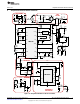
LINE NEUT V+ R26 R29 R32 R39 R48 L1 C7 R62 L4 R24 C17 R33 R20 R8 C9 R9 R56 1 V+ D2 D6 D3 D7 RETURN BIAS ZCD VCC GATE GND CS ISEN R5 R7 Q1 R44 L2 R51 D25 D8 Q11 C22 R15 R14 R45 ZCD J8 16 BIAS 15 14 R61 J13 13 PBIAS 12 10 11 9 R1 Q2 Sbias R11 R49 Flyback PFC C3 R47 R3 C66 PBIAS C1 R2 C2 R10 R60 ZCD R17 D9 R59 C44 C42 D16 Q20 C29 D5 R42 COMP R41 FB Q3 R30 R34 D1 1 2 3 4 5 40 40 10 . T1 . . .
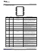
120V Bill of Materials www.ti.com 12 120V Bill of Materials Table 1. 120V Bill of Materials Reference Designator Part Value Manufacturer Part Number C1 CAP MPY 0.22µF 400V RAD WIMA MKP10-.22/400/20 C2, C3, C8, C9, C30, C66 CAP CER 0.22µF 250V RAD TDK FK20X7R2E224K C4, C44 CAP ELEC 220µF 35V RAD NICHICON UHE1V221MPD C5, C23, C42, C46 CAP CER 0.
120V Bill of Materials www.ti.com Table 1. 120V Bill of Materials (continued) R10 RES 40.2Ω 1% 0.25W 1206 VISHAY CRCW120640R2FKEA R12, R14, R15 RES 301Ω 1% 0.25W 1206 VISHAY CRCW1206301RFKEA R16 RES 6.04kΩ 1% 0.125W 0805 VISHAY CRCW08056K04FKEA R17 RES 100kΩ 1% 0.1W 0603 VISHAY CRCW0603100KFKEA R19, R41, R43, R61, R73 RES 0Ω 5% 0.1W 0603 VISHAY CRCW06030000Z0EA R20 RES 499kΩ 1% 0.1W 0603 VISHAY CRCW0603499KFKEA R21, R69 RES 20.0kΩ 1% 0.
230V Bill of Materials www.ti.com 13 230V Bill of Materials Table 2. 230V Bill of Materials Reference Designator Part Value Manufacturer Part Number C1 CAP MPY 0.062µF 1000V RAD VISHAY BFC238330623 C2, C3, C8, C9, C30, C66 CAP CER 0.1µF 630V RAD TDK FK22X7R2J104K C4, C44 CAP ELEC 220µF 35V RAD NICHICON UHE1V221MPD C5, C23, C42, C46 CAP CER 0.
230V Bill of Materials www.ti.com Table 2. 230V Bill of Materials (continued) R6, R11 RES 10Ω 1% 0.25W 1206 VISHAY CRCW120610R0FKEA R8, R9, R56 RES 2.4kΩ 5% 1W 2512 VISHAY CRCW25122K40JNEG R10 RES 40.2Ω 1% 0.25W 1206 VISHAY CRCW120640R2FKEA R12, R14, R15 RES 301Ω 1% 0.25W 1206 VISHAY CRCW1206301RFKEA R16 RES 6.04kΩ 1% 0.125W 0805 VISHAY CRCW08056K04FKEA R17 RES 100kΩ 1% 0.1W 0603 VISHAY CRCW0603100KFKEA R19, R41, R43, R61, R73 RES 0Ω 5% 0.
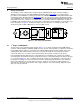
PCB Layout www.ti.com 14 PCB Layout Figure 26. Top Copper and Silkscreen Figure 27.
IMPORTANT NOTICE Texas Instruments Incorporated and its subsidiaries (TI) reserve the right to make corrections, enhancements, improvements and other changes to its semiconductor products and services per JESD46, latest issue, and to discontinue any product or service per JESD48, latest issue. Buyers should obtain the latest relevant information before placing orders and should verify that such information is current and complete.