
User manual

www.ti.com
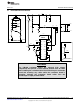
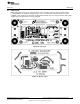
PCB Layout
17 PCB Layout
NOTE: Spacing between traces and components of this evaluation board are based on high voltage
recommendations for designs that will be potted. Users are cautioned to satisfy themselves as to the
suitability of this design for the intended end application and take any necessary precautions where high
voltage layout and spacing rules must be followed.
Figure 36. Top Layer
Figure 37. Bottom Layer
27
SNOA559B–October 2011–Revised May 2013 AN-2127 LM3448 A19 Edison Retrofit Evaluation Board
Submit Documentation Feedback
Copyright © 2011–2013, Texas Instruments Incorporated