
User manual

www.ti.com
Design Guide
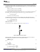
Re-circulating Diode
The main re-circulating diode (D4) should be sized to block the maximum reverse voltage V
RD4(MAX)
,
operate at the maximum peak I
DR-PK(MAX)
and RMS currents I
D4-RMS(MAX)
, and dissipate the maximum power
P
D4(MAX)
as determined by the following equations,
(20)
(21)
(22)
(23)
NOTE: For proper converter operation, the chosen diode should have a reverse recovery time that is less
than the LM3448's leading edge blanking time of 125ns.
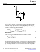
13.2 Bias Supplies and Capacitances
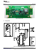
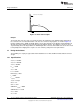
The VCC bias supply circuit is shown in Figure 33. The passFET (Q1) is used in its linear region to stand-
off the line voltage from the LM3448 regulator. Both the VCC startup current and discharging of the EMI
filter capacitance for proper phase angle detection are handled by Q1. Therefore Q1 has to block the
maximum peak input voltage and have both sufficient surge and power handling capability with regards to
its safe operating area (SOA). The design equations are,
(24)
(25)
(26)
Note that if additional TRIAC holding current is to be sourced through Q1, then the transistor will need to
be sized appropriately to handle the additional current and power dissipation requirements.
17
SNOA559B–October 2011–Revised May 2013 AN-2127 LM3448 A19 Edison Retrofit Evaluation Board
Submit Documentation Feedback
Copyright © 2011–2013, Texas Instruments Incorporated